Transcription of Freewheeling Diode Reverse Recovery Failure Modes in IGBT ...
1 Freewheeling Diode Reverse Recovery Failure Modes in IGBT Applications Rahimo and Shammas Institute of Electrical and Electronics Engineers, March/April 2001 Copyright [2001] IEEE. Reprinted from the IEEE Transactions on Industry Applications, vol. 37. This material is posted here with permission of the IEEE. Such permission of the IEEE does not in any way imply IEEE endorsement of any of ABB Switzerland Ltd, Semiconductors's products or services. Internal or personal use of this material is permitted. However, permission to reprint/republish this material for advertising or promotional purposes or for creating new collective works for resale or redistribution must be obtained from the IEEE by writing to ABB Switzerland Ltd.
2 Freewheeling Diode Reverse Recovery Failure Modes in IGBT Applications IEEE Page 1 of 10 March/April 2001 Freewheeling Diode Reverse Recovery Failure Modes in IGBT Applications Rahimo and Shammas Abstract- In this paper, Reverse Recovery Failure Modes in modern fast power diodes are investigated. By the aid of semiconductor device simulation tools, a better view is obtained for the physical process, and operating conditions at which both Diode snappy Recovery and dynamic avalanching occur during the Recovery period in modern high frequency power electronic applications. The work presented here confirms that the Reverse Recovery process can by expressed by means of Diode capacitive effects which influence the Reverse Recovery characteristics.
3 The paper also shows that the control of the carrier gradient and the remaining stored charge in the drift region during the Recovery phase influence both Failure Modes and determine if the Diode exhibits a soft, snappy or dynamic avalanche Recovery characteristics. I. INTRODUCTION THE RISE of the converter frequency in power electronics requires fast power semiconductor devices with low switching losses during the transient periods. Today, Mos-Bipolar Transistors such as the (IGBT) present interesting characteristics combining both MOS and bipolar structures to achieve a voltage driven device with low on-state losses, low switching losses and a high current density capability.
4 These devices are increasingly used in many modern converter applications, but their optimum performances are often restricted by the Freewheeling Diode Reverse Recovery characteristics. The Freewheeling Diode has always been said to be the weak component in many applications because it reduces the switching speed of the IGBT during the turn-on transient period. The main two Reverse Recovery Failure Modes in diodes operating under high stress condition are 1- Snappy Recovery . 2- Reverse Recovery Dynamic Avalanche. One of the most common and catastrophic Failure Modes in fast diodes is due to Diode snappy Recovery . Previous work have shown that under adverse combinations of high commutating di/dt, large circuit stray inductance, low forward current and low junction temperature, it is likely that all fast power diodes produce excessive voltage spikes due to snappy Recovery [1].
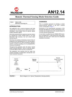
5 This in turn can destroy the Diode and ultimately cause a circuit Failure due to excessive inrush duty in the Recovery period. Experimental results are shown comparing a desirable soft Recovery performance in figure (1-a) to snappy Recovery in figure (1-b). Snappy Recovery of fast power PIN diodes has been investigated over the years [2]. These studies have shown that the depletion of the remaining stored charge during the Recovery period results in a current discontinuity (chop-off). This produces a very high dir/dt and hence a large voltage overshoot which may result in the destruction of the device. The second type of Failure mode, termed as Reverse Recovery dynamic avalanching occurs at high di/dt switching speeds.
6 Normally, the process itself is safe if the device does not exhibit any non-uniformaties in the Recovery current. However, dynamic avalanching can result in the generation of a hot spot in the silicon die due to non-uniform current crowding leading to the distruction of the device as shown in figure (1-c). The causes of these hot spots can range from process to material variations in a single Diode silicon chip. To prevent this Failure mode, certain design/process consideration must be taken into account to minimise the effects of any current non-uniformaties. VoltageCurrent (a) soft Recovery CurrentVoltageVoltage Spike (b) snappy Recovery ABB Switzerland Ltd.
7 Freewheeling Diode Reverse Recovery Failure Modes in IGBT Applications IEEE Page 2 of 10 March/April 2001 CurrentVoltageVoltage Collapse (c) dynamic Avalanche Fig. 1 Reverse Recovery waveforms for a fast Diode , (a) soft Recovery , (b) snappy Recovery and (c) dynamic avalanching. These Diode Failure Modes can destroy the IGBT and ultimately cause a circuit Failure due to excessive inrush duty in the Recovery period as shown in figure (2). The purpose of this investigation is to gain a better understanding of the physical process, and causes of these Failure Modes in modern fast power diodes. VceIcDiode Reverse Recovery FailureIGBT Short Circuit Overcurrent Failuredi/dtdi /dtr Fig.
8 2 Freewheeling Diode Reverse Recovery Failure during IGBT turn-on. II. Diode Reverse Recovery PROCESS Figure (3-a) shows typical Diode current and voltage waveforms during Reverse Recovery , while figure (3-b) shows the associated excess minority carrier distribution (hole density) and space charge spreading in the drift region during Reverse Recovery . FC t0 VRIFC urrentVoltageVprIprdi/dtrdi /dtdv/dttimet1t2t3t4t5Ph1 Ph2 Ph3 Ph4 Ph5 RB (a) Diode Reverse Recovery voltage and current waveforms. Hole densitySpace charge P+N-N+t0t1t2t3t4t5n (x)eX- d+ d (b) Excess carrier distribution during Reverse Recovery . Fig.
9 3 Reverse Recovery Characteristics (a) with the associated excess minority carrier distributions (b). During Forward Conduction FC, the Diode conducts a constant steady state forward current IF, and a fixed forward voltage drop Vf appears across the Diode . An increase in the Diode current will lead to an increase in the number of excess minority carriers associated with a larger conductivity modulation in the drift region. The current flows only due to recombination and generation processes where the total stored charge in the drift region is a function of the current density, carrier lifetime, junction temperature and carrier injection efficiency.
10 The excess minority carrier distribution in the drift region [3] is given as nxIqALeFaeffa()=t2[cosh(/)sinh(/)sinh(/) cosh(/)xLdLBxLdLaaaa-] (1) where the boundary conditions are given as (- +--+dxdpnnn.) (2) La is the ambipolar diffusion coefficient, ta is the ambipolar lifetime value, B is the hole to electron mobility ratio (B 3) and (d=WB / 2) where WB is the drift region total thickness. When the Diode is subjected to a Reverse voltage VR at tt=0, a certain Reverse Recovery transient period elapses before the Diode can reach its full Reverse Blocking RB state. This period can be divided into five phases : Phase 1 (Commutating Phase): This phase begins with the application of the Reverse voltage VR at tt=0.