Transcription of Power MOSFET Basics - IXYS Corporation
1 IXAN0061 1 Power MOSFET Basics Abdus Sattar, IXYS Corporation Power mosfets have become the standard choice for the main switching devices in a broad range of Power conversion applications. They are majority carrier devices with no minority carrier injection, superior to Power Bipolar Junction Transistors (BJTs) and Insulated Gate Bipolar Transistors (IGBTs) in high frequency applications where switching Power losses are dominant. They can be paralleled because the forward voltage drops with increasing temperature, ensuring an even distribution of current among all components. The major categories of Power mosfets are: 1.
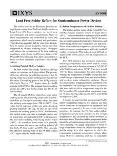
2 N-Channel Enhancement-Mode Power MOSFET 2. P-Channel Enhancement-Mode Power MOSFET 3. N-Channel Depletion-Mode Power MOSFET N-channel enhancement-mode is the most popular for use in Power switching circuits because of low on-state resistance compared to P-channel devices. An N-channel depletion-mode Power MOSFET differs from the enhancement-mode in that it is normally ON at 0V gate bias and requires a negative gate bias to block current [2]. Vertical DMOS Structure A simplified vertical DMOS Power MOSFET with four layers of n+pn-n+ structure is termed as N-Channel Enhancement-Mode Power MOSFET shown in Figure 1.
3 A positive gate voltage (Vgs), higher than the gate threshold level (Vgs(th)) will create an n-type inversion channel under the gate oxide, connecting the source to the drain and allowing a current to flow. The gate threshold voltage is defined as the minimum gate bias required for creating the n-type inversion channel under the gate oxide. Power MOSFET has a parasitic BJT and an intrinsic body diode as integral parts of its structure as shown in Figure 1 [2]. Figure 1: N-Channel Enhancement-Mode Power MOSFET Structure [2] IXAN0061 2 Intrinsic Components Parasitic BJT: Power MOSFET has a parasitic BJT as an integral part of its structure as shown in Figure 1.
4 The body region serves as the base, the source as the emitter and the drain as the collector. It is important to keep this BJT OFF of all times by keeping the potential of the base as close to the emitter potential as possible. This is accomplished by shorting the body and the source part of the MOSFET . Otherwise, the potential at the base would turn on the BJT and lead the device into the latchup condition, which would destroy the device [2]. Body Diode: An intrinsic body diode is formed in the body-drain p-n junction connected between the drain and source as shown in Figure 1. Figure 2 shows the circuit symbols for both N-channel and P-channel enhancement types Power mosfets .
5 Figure 2: (a) N-channel (b) P-channel enhancement-mode Power MOSFET The body diode is convenient in circuits that require a path for the reverse drain current (called free wheeling current ) such as half-bridge and full-bridge converter circuits in motor control applications [2]. Power MOSFET Characteristics Static Behavior The static behavior is defined by the output characteristics, on-resistance, and the transconductance of the device. Output Characteristics: The output characteristics for an N-channel enhancement-mode Power MOSFET with the drain current (Ids) as a function of drain-source voltage (Vds) with gate-source voltage (Vgs) as a parameter are shown in Figure 3.
6 IXAN0061 3 Figure 3: N-channel enhancement-mode Power MOSFET I-V Characteristics It has regions labeled as Ohmic, Current-Saturated and Cut-off. In the Cut-off region, the gate-source voltage (Vgs) is less than the gate-threshold voltage (Vgs(th)) and the device is an open-circuit or Off. In the Ohmic region, the device acts as a resistor with almost a constant on-resistance, (RDS(on)) defined by Vds /Ids. In the current-saturated region, the drain current is a function of the gate-source voltage and defined by, )()()(2)(thgsgsfsthgsgsdsVVgVVKI = = Equation (1) where K is a parameter depending on the temperature and device geometry and gfs is the current gain or transconductance of the device.
7 When the drain voltage (Vds) is increased, the positive drain potential opposes the gate voltage bias and reduces the surface potential in the channel. The channel inversion layer charge decreases with increasing Vds and ultimately, it becomes zero when the drain voltage equals to)()(thgsgsVV . This point is called the channel pinch-off point where the drain current becomes saturated [2]. On-resistance RDS (on): The on-resistance determines the conduction Power dissipation and increases with increasing temperature as shown in Figure 4. IXAN0061 125 150TJ - Degrees Cent i gradeR D S ( o n ) - NormalizeID = 22 AID = 11 AVGS = 10V Figure 4.
8 Increase on-resistance RDS (on) with temperature TJ for Power MOSFET The on-resistance can be defined by, wcmlsubDJAchSourceonDSRRRRRRRR++++++=)( Equation (2) Where, SourceR= Source diffusion resistance chR= Channel resistance AR= Accumulation resistance JR= JFET component-resistance of the region between the two-body regions DR= Drift region resistance subR= Substrate resistance wcmlR=Sum of Bond Wire resistance, the Contact resistance between the source and drain metallization and leadframe contributions. The temperature coefficient of RDS (on) is positive because of majority-only carrier movement.
9 It is a useful property, which ensures thermal stability when paralleling the devices. Transconductance gfs: The Transconductance is defined as the change in drain current divided by the change in gate voltage for a constant drain voltage: tconsdsgsDfsVdVdIgtan== Equation (3) A large transconductance is desirable to obtain a high current handling capability with low gate drive voltage and for achieving high frequency response. A typical variation of transconductance as a function of drain current is shown in Figure 5.
10 The reduction in the mobility with increasing temperature severely affects the transconductance of Power MOSFET . IXAN0061 5020406080100120140050100150200250300350 I D - Amperesg f s - SiemensTJ = -40 C 25 C 150 C Figure 5: Transconductance vs the Drain Current [2] Dynamic Behavior The dynamic behavior is described by the switching characteristics of Power MOSFET . The intrinsic capacitances, resistance, gate charge and the reverse recovery characteristics of the body diode play significant role in the dynamic performance of the device. Intrinsic Capacitances: Power MOSFET s dynamic behavior depends on the intrinsic resistance and capacitance, which has components as gate-to-source capacitance (Cgs), gate-to-drain capacitance (Cgd) and drain-to-source capacitance (Cds) as shown in Figure 6.