Example: marketing
HMC833LP6GE - Analog Devices
VCO Open Loop Phase Noise at fo @3 GHz/30 = 100 MHz 10 kHz Offset -112 dBc/Hz 100 kHz Offset -142 dBc/Hz 1 MHz Offset -165 dBc/Hz 10 MHz Offset -168 dBc/Hz 100 MHz Offset -171 dBc/Hz VCO Open Loop Phase Noise at 2fo @ 4 GHz 10 kHz Offset -80 dBc/Hz 100 kHz Offset -110 dBc/Hz 1 MHz Offset -135 dBc/Hz 10 MHz Offset -155 dBc/Hz 100 MHz Offset -162 ...
Tags:
Information
Domain:
Source:
Link to this page:
Documents from same domain

AD743 Ultralow Noise BiFET Op Amp Data Sheet …
www.analog.comREV. E Information furnished by Analog Devices is believed to be accurate and reliable. However, no responsibility is assumed by Analog Devices for its

MT-070: In-Amp Input RFI Protection - Analog …
www.analog.comRev.0, 10/08, WK Page 1 of 6 MT-070 TUTORIAL In-Amp Input RFI Protection . PROTECTING IN-AMPS AGAINST RFI . Real-world applications must deal with an ever increasing amount of radio frequency

LTC3108 - Ultralow Voltage Step-Up Converter and …
www.analog.comLTC3108 3108fc For more information www.linear.com/LTC3108 LDO

1.8 V Low Power CMOS Rail-to-Rail Input/Output …
www.analog.com1.8 V Low Power CMOS Rail-to-Rail Input/Output Operational Amplifier Data Sheet AD8515 Rev. E Document Feedback Information furnished by Analog Devices is believed to be accurate and reliable.

Low Cost Micropower, Low Noise CMOS Rail-to …
www.analog.comLow Cost Micropower, Low Noise CMOS Rail-to-Rail, Input/Output Operational Amplifiers Data Sheet AD8613/AD8617/AD8619 Rev. H Document Feedback Information furnished by Analog Devices is believed to be accurate and reliable.

Low Cost CMOS, High Speed, Rail-to-Rail Amplifiers
www.analog.comLow Cost CMOS, High Speed, Rail-to-Rail Amplifiers Data Sheet ADA4891-1/ADA4891-2/ADA4891-3/ADA4891-4 Rev. F Document Feedback Information furnished by Analog Devices ...

Zero-Drift, Single-Supply, Rail-to-Rail Input/Output ...
www.analog.comZero-Drift, Single-Supply, Rail-to-Rail Input/Output Operational Amplifier Data Sheet AD8628/AD8629/AD8630 FEATURES Lowest auto-zero amplifier noise Low offset voltage: 1 µV AD8628

FEATURES DESCRIPTIO U - analog.com
www.analog.com1 LT1025 1025fb DESCRIPTIO U APPLICATIO S U 80µA Supply Current 4V to 36V Operation 0.5°C Initial Accuracy (A Version) Compatible with Standard Thermocouples (E, J, K, R, S, T) Auxiliary 10mV/°C Output Available in 8-Lead PDIP and SO Packages Thermocouple Cold Junction Compensator Centigrade Thermometer Temperature …

LT1173 - Micropower DC/DC Converter Adjustable …
www.analog.comLT1173 1 Micropower DC/DC Converter Adjustable and Fixed 5V, 12V VOUT 5V/DIV 0V PROGRAM 5V/DIV 5ms/DIV 1173 TA02 L1* 100µH LT1173 • TA01 + GND SW2 FB SW1 ILIM VIN 10 F LT1173

AD9850 CMOS, 125 MHz Complete DDS …
www.analog.comrev. h a cmos, 125 mhz complete dds synthesizer ad9850 functional block diagram clock out clock out analog in analog out dac rset …
Related documents
Microwave Wideband Synthesizer with Integrated VCO Data ...
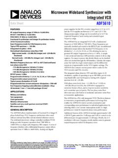
www.analog.comMicrowave radio . GENERAL DESCRIPTION The ADF5610 allows implementation of fractional-N or Integer N phase-locked loop (PLL) frequency synthesizers when used with an external loop filter and an external reference source. The wideband microwave voltage controlled oscillator (VCO) designpermits frequency operation from 7300 MHz to
Diodes and Transistors
inst.eecs.berkeley.edu(phase-locked loop) and FLL (frequency-locked loop) circuits, allowing tuning circuits, such as those in television receivers, to lock quickly, replacing older designs that took a long time to warm up and lock.. Zener diodes Diodes that can be made to …
High Frequency VCO Design and Schematics
www.qsl.netcontained within a phase-locked loop and the frequency of modulation lies within the closed-loop bandwidth, unwanted interactions can result. One of the most serious load pulling situations that can occur in practice arises in modulators where the modulation signal causes (low-frequency) baseband frequency modulation of the load.
EMBEDDED SYSTEMS PROGRAMMING WITH THE PIC16F877
academic.csuohio.eduPLL = Phase-Locked Loop POR = Power-On Reset PROM = Programmable Read Only Memory PSP = Parallel Slave Port PWM = Pulse Width Modulation Q = Flip-Flop, Counter, or Shift Register Output State (Data Out) RAM = Random Access Memory (A Read/Write Memory) RC = Resistor/Capacitor (Time Constant or Circuit)

Phase Locked Loops (PLL) and Frequency Synthesis
rfic.eecs.berkeley.eduPhase Locked Loops A PLL is a truly mixed-signal circuit, involving the co-design of RF, digital, and analog building blocks. A non-linear negative feedback loop that locks the phase of a VCO to a reference signal. Applications include generating a clean, tunable, and stable reference (LO) frequency, a process referred to as frequency synthesis
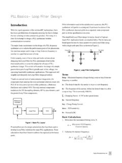
PLL Basics–Loop Filter Design
www.am1.usLoop Filters to be used in many of today's PLL applications. Figure 4 shows the excellent Phase Noise performance of the RF PLL of Fujitsu’s new MB15F08SL dual 2.5/1.1 GHz PLL using the calculated Loop Filter values. Marker “0” shows the Phase Noise inside the loop is –80.5 dBc/Hz. Marker “1” shows the loop bandwidth is 16000 Hz ...