Transcription of HMC849ALP4CE - Analog Devices
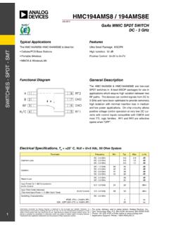
1 SWITCHES - SPDT - ISOLATION SPDTNON-REFLECTIVE SWITCH, DC - 6 GHzFor price, delivery, and to place orders: Analog Devices , Inc., One Technology Way, Box 9106, Norwood, MA 02062-9106 Phone: 781-329-4700 Order online at Support: Phone: 1-800- Analog -DInformation furnished by Analog Devices is believed to be accurate and reliable. However, no responsibility is assumed by Analog Devices for its use, nor for any infringements of patents or other rights of third parties that may result from its use. Specifications subject to change without notice. No license is granted by implication or otherwise under any patent or patent rights of Analog Devices . Trademarks and registered trademarks are the property of their respective owners. General DescriptionFeaturesFunctional DiagramHigh Isolation: up to 60 dBSingle Positive Control: 0/+3V to +5 VHigh Input IP3: +52 dBm Non-Reflective Design All Off State16 Lead 4x4 mm QFN Package: 16 mm Typical ApplicationsThe HMC849 ALP4CE is ideal for: Cellular/4G Infrastructure WiMAX, WiBro & Fixed Wireless Automotive Telematics Mobile Radio Test EquipmentThe HMC849 ALP4CE is a high isolation non-reflec- tive DC to 6 GHz GaAs pHEMT SPDT switch in a low cost leadless surface mount package.
2 The switch is ideal for cellular/WiMAX/4G Infrastructure applicati- ons yielding up to 60 dB isolation, low dB inser-tion loss and +52 dBm input IP3. Power handling is excellent up through the 5 - 6 GHz WiMAX band with the switch offering a P1dB compression point of +31 dBm. On-chip circuitry allows a single positive voltage control of 0/+3V or 0/+5V at very low DC currents. An enable input (EN) set to logic high will put the switch in an all off Specifications, TA = +25 C, Vctl = 0/Vdd, Vdd = +3V to +5V, 50 Ohm LossDC - - - (RFC to RF1/RF2)DC - - - GHz534835605650dBdBReturn Loss (On State)DC - - GHz1714dBdBReturn Loss (Off State)DC - GHz15dBInput Power for 1 dB Compression+3V+ - GHz24302733dBmdBmInput Third Order Intercept(Two-Tone Input Power = +10 dBm Each Tone)DC - GHz52dBmSwitching SpeedtRISE, tFALL (10/90% RF)tON, tOFF (50% CTL to 10/90% RF)DC - GHz60150600nsnsSWITCHES - SPDT - ISOLATION SPDTNON-REFLECTIVE SWITCH, DC - 6 GHzFor price, delivery, and to place orders: Analog Devices , Inc.
3 , One Technology Way, Box 9106, Norwood, MA 02062-9106 Phone: 781-329-4700 Order online at Support: Phone: 1-800- Analog -DReturn Loss [1]Insertion Loss Isolation BetweenPorts RFC and RF1 / and 1 dB Input Compression Point, Vdd = 5V, and 1 dB Input Compression Point, Vdd = 3V, LinearIsolation Between Ports RF1 and RF2[1] RFC is reflective in all off +25C+85C -40 CINSERTION LOSS (dB)FREQUENCY (GHz)-100-80-60-40-20001234567RF1RF2 ALL OFFISOLATION (dB)FREQUENCY (GHz) dB Compression Point1dB Compression PointINPUT COMPRESSION (dBm) FREQUENCY (GHz) dB Compression Point1 dB Compression PointINPUT COMPRESSION (dBm) FREQUENCY (GHz)-40-35-30-25-20-15-10-5001234567 RFCRF1, RF2 OFFRF1, RF2 ONRETURN LOSS (dB)FREQUENCY (GHz)-80-70-60-50-40-30-20-10001234567 RFC-RF1 ONRFC-RF2 ONISOLATION (dB)FREQUENCY (GHz)SWITCHES - SPDT - ISOLATION SPDTNON-REFLECTIVE SWITCH, DC - 6 GHzFor price, delivery, and to place orders.
4 Analog Devices , Inc., One Technology Way, Box 9106, Norwood, MA 02062-9106 Phone: 781-329-4700 Order online at Support: Phone: 1-800- Analog -DInput Third Order Intercept Point, Vdd = 5 VInput Third Order Intercept Point, Vdd = 5V, LinearInput Third Order Intercept Point, Vdd = 3 VInput Third Order Intercept Point, Vdd = 3V, +25C+85C -40 CIP3 (dBm)FREQUENCY (GHz) in log scale40455055600123456+25C+85C -40 CIP3 (dBm)FREQUENCY (GHz) +25C+85C -40 CIP3 (dBm)FREQUENCY (GHz) in log scale40455055600123456+25C+85C -40 CIP3 (dBm)FREQUENCY (GHz) and 1 dB Input Compression Point, Vdd = and 1 dB Input Compression Point, Vdd = dB Compression Point1 dB Compression PointINPUT COMPRESSION (dBm) FREQUENCY (GHz) in log dB Compression Point1 dB Compression PointINPUT COMPRESSION (dBm) FREQUENCY (GHz) in log scaleSWITCHES - SPDT - ISOLATION SPDTNON-REFLECTIVE SWITCH, DC - 6 GHzFor price, delivery, and to place orders: Analog Devices , Inc.
5 , One Technology Way, Box 9106, Norwood, MA 02062-9106 Phone: 781-329-4700 Order online at Support: Phone: 1-800- Analog -DTruth TableAbsolute Maximum RatingsControl InputSignal Path StateVctlENRFC - RF1 RFC - RF2 LowLowOFFONHighLowONOFFLowHighOFFOFFHigh HighOFFOFFD igital Control VoltagesStateBias ConditionLow0 to + Vdc @ <1 A TypicalHigh+ to + Vdc @ 40 A TypicalBias Voltage (Vdd)7 VControl Voltage (Vctl, EN)-1V to Vdd +1 VRF Input Power *Through Path 3V/5 VTermination Path 3V/5V31 / 33 dBmChannel Temperature150 CContinuous Pdiss (T = 85 C) (derate mW/ C for through path, and mW/ C for termination path above 85 C)Through PathTermination WThermal Resistance (channel to package bottom)Through PathTermination Path6 C / C/ WStorage Temperature-65 to +150 COperating Temperature-40 to +85 CESD Sensitivity (HBM)Class 1A* The RF input power is quite lower than the breakdown power levels.
6 Hence, the only concern with this product is the thermal (V)I d d ( Ty p.)(mA) Voltage & CurrentELECTROSTATIC SENSITIVE DEVICEOBSERVE HANDLING PRECAUTIONSSWITCHES - SPDT - ISOLATION SPDTNON-REFLECTIVE SWITCH, DC - 6 GHzFor price, delivery, and to place orders: Analog Devices , Inc., One Technology Way, Box 9106, Norwood, MA 02062-9106 Phone: 781-329-4700 Order online at Support: Phone: 1-800- Analog -DOutline DrawingPart NumberPackage Body MaterialLead FinishMSL RatingPackage Marking [1]HMC849 ALP4 CERoHS-compliant Low Stress Injection Molded Plastic100% matte SnMSL3 [2]H849 AXXXX[1] 4-Digit lot number XXXX[2] Max peak reflow temperature of 260 CPackage InformationNOTES:1. LEADFRAME MATERIAL: COPPER ALLOY2. DIMENSIONS ARE IN INCHES [MILLIMETERS]3. LEAD SPACING TOLERANCE IS PAD BURR LENGTH SHALL BE MAXIMUM.
7 PAD BURR HEIGHT SHALL BE PACKAGE WARP SHALL NOT EXCEED ALL GROUND LEADS AND GROUND PADDLE MUST BE SOLDERED TO PCB RF REFER TO HITTITE APPLICATION NOTE FOR SUGGESTED L AND PAT - SPDT - ISOLATION SPDTNON-REFLECTIVE SWITCH, DC - 6 GHzFor price, delivery, and to place orders: Analog Devices , Inc., One Technology Way, Box 9106, Norwood, MA 02062-9106 Phone: 781-329-4700 Order online at Support: Phone: 1-800- Analog -DPin DescriptionsApplication CircuitPin NumberFunctionDescriptionInterface Schematic1 VddSupply input. See truth and control voltage , 9, 12 RFC, RF1, RF2 These pins are DC coupled and matched to 50 Ohms. Blocking capacitors are , 6, 7, 8,13, 14, 15, 16N/CThe pins are not connected internally; however, all data shown herein was measured with these pins connected to RF/DC ground See truth and control voltage , 11 GNDP ackage bottom must also be connected to PCB RF - SPDT - ISOLATION SPDTNON-REFLECTIVE SWITCH, DC - 6 GHzFor price, delivery, and to place orders: Analog Devices , Inc.
8 , One Technology Way, Box 9106, Norwood, MA 02062-9106 Phone: 781-329-4700 Order online at Support: Phone: 1-800- Analog -DEvaluation PCB The circuit board used in the final application should be generated with proper RF circuit design techniques. Signal lines at the RF port should have 50 Ohm impedance and the package ground leads and backside ground slug should be connected directly to the ground plane similar to that shown above. The evaluation circuit board shown above is available from Analog Devices , upon of Materials for Evaluation PCB EV1 HMC849 ALP4C [1]ItemDescriptionJ1 - J3PC Mount SMA RF ConnectorJ4 - J8DC PinC1 - C4100 pF Capacitor, 0402 SPDT SwitchPCB [2]106965 Evaluation PCB[1] Reference this number when ordering complete evaluation PCB[2] Circuit Board Material: Rogers 4350 or Arlon 25 FRSWITCHES - SPDT - ISOLATION SPDTNON-REFLECTIVE SWITCH, DC - 6 GHzFor price, delivery, and to place orders: Analog Devices , Inc.
9 , One Technology Way, Box 9106, Norwood, MA 02062-9106 Phone: 781-329-4700 Order online at Support: Phone: 1-800- Analog -DNotes.