Transcription of Two-Resistor Model for Thermal Simulation - Rohm
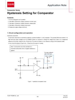
1 1/4 2017 ROHM Co., Ltd. No. 60AP001E 2020 ROHM Co., Ltd. No. 62AN156E APRIL 2020 Application Note Power Devices Two-Resistor Model for Thermal Simulation This application note explains the Two-Resistor Model , which is the simplest Model among Thermal models used in Thermal simulations. The Thermal simulations mentioned here cover three-dimensional Model Thermal conduction and Thermal fluid analysis tools. Models for Thermal simulations As shown in Figure 1, the models for Thermal simulations can be classified into two types: compact Thermal Model (CTM) and detailed Model . For the CTM, JEDEC Solid State Technology Association has standardized two types of Thermal models. The Two-Resistor Model is suitable for discrete and LSI devices. Since this simple Model is structured only by vertically dividing a package at the junction, it is ideal for single function devices such as discrete products.
2 In addition, although the analysis speed of simulations is fast thanks to the simplicity of the Model , its precision is the lowest among the three models. The DELPHI Model supports LSI as well. It represents a package with a multi- resistor network so that errors can uniformly be reduced in a variety of operating environments. This Model achieves a relatively good balance between analysis speed and precision with a small number of elements. However, it does not support the transient Thermal analysis. Type Compact Thermal Model (CTM) Detailed Model Two-Resistor Model DELPHI Model Standard JESD15-3 JESD15-4 Shape Case NodeBoard NodeJunctionNode JCtop JB Top InnerTop OuterBottom InnerBottom OuterLeadsJunction(heat source)ThermalResistors Summary Simple Model only dividing a package vertically at the junction Ideal for single function devices such as discrete products Model representing a package with a multi- resistor network Detailed Model including details of dimensions and physical properties of materials Precision Good Better Best Shortcomings Least precise among the 3 models Transient analysis not supported Transient analysis not supported Variation in quality without any standard Long Simulation time No compatibility between tools Figure 1.
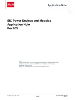
3 Models for Thermal simulations 2/4 2020 ROHM Co., Ltd. No. 62AN156E APRIL 2020 Application Note Two-Resistor Model for Thermal Simulation In contrast, there is no standard for the detailed models and the quality of models varies with the companies that created them. Details of dimensions and physical properties of materials are needed to create a Model . A non-disclosure agreement is normally required to obtain such information. Although the detailed Model has the best precision, its Simulation takes time. In addition, the Thermal analysis tools are not compatible since there is no standard. Description of Two-Resistor Model The physical arrangement of the Two-Resistor Model is composed of three nodes as shown in Figure 2. The package includes a single integrated circuit. The temperature is represented with a single temperature node.
4 The Thermal flow path is represented using a Thermal resistance network. Junction Node, Case Node, and Board Node represent the Thermal source of the chip, the upper surface of the package, and the circuit board temperature at a position of 1 mm from the edge of the device, respectively. Two Thermal resistors are connected between the junction and the case and between the junction and the board. The values of these Thermal resistances are generated based on the Thermal test of the JEDEC Standard. If no measurement value is available, the values extracted from the verified detailed Model that simulates the test environment are used. For the extraction from the detailed Model , three-dimensional Thermal fluid analysis tools, such as Simcenter Flotherm *1, are used. The heating power occurs on Junction Node.
5 Case Node is considered to be in direct Thermal contact with the environment immediately above the top part of the package (normally, air or Thermal conducting material used together with the heat sink). Board Node is considered to be in direct Thermal contact with the environment immediately below the footprint of the package (normally, the printed circuit board). The heat from the Thermal source of the chip flows in two directions. One flows as radiation and convective heat transfer from the upper surface of the package to the surroundings, or into the heat sink mounted on the top of the package. The other flows into the PCB from the back surface of the package and the lead. Furthermore, no Thermal flow is considered to be transferred from the side surfaces of the package to the surrounding fluid in this Model .
6 Case NodeBoard NodeJunctionNode JCtop JB Figure 2. Physical arrangement of Two-Resistor Thermal Model Overview of Thermal resistance test environment The methods of Thermal resistance measurement are described for JB in JEDEC Standard JESD51-8 and for JC in JESD51-14. Here, an overview of the test environment for the two Thermal resistors is explained. See JEDEC Standards for more details. Test environment for JB For the measurement of JB, an environment where the heat generated on Junction Node can be transferred to the board side is used. Figure 3 shows the schematic diagram of the test environment. The ring type cold plate is cooled with fluid (mainly water). The circuit board is clamped with the cold plate from both sides so that heat from the package flows radially in the inner surface of the circuit board.
7 In addition, Thermal insulation material is used for the package openings on the top and bottom of the cold plate to block the ambient temperature. The circuit board temperature is measured with the thermocouple. The temperature monitoring point is at the center of one side of the package, and within 1 mm from the periphery. *1: Simcenter Flotherm is a trademark of Siemens Industry Software Inc. 3/4 2020 ROHM Co., Ltd. No. 62AN156E APRIL 2020 Application Note Two-Resistor Model for Thermal Simulation After applying the power to the device, the junction temperature and the circuit board temperature are measured in a steady state. JB is determined by Equation (1). [ / ] (1) TJ: Junction temperature when the device reaches the steady state after Power P is applied [ C] TB: Circuit board temperature in the steady state [ C] P: Power consumption that causes the change in the junction temperature [W] Test environment for JC As described in MIL-STD-883E, JC had traditionally been determined by directly measuring the temperature difference between the junction and the surface of the case in contact with the water cooled copper heat sink using a thermocouple.
8 Since the measurement of the case temperature with a thermocouple is prone to errors, these results had a poor reproducibility. This is because the contact between the thermocouple and the case may not be at the maximum case temperature due to the latent temperature distribution in the package case. In addition, the temperature may be lowered if the thermocouple is not adequately insulated from the cold plate. In JESD51-14, the reproducibility of JC measurement is significantly improved by eliminating the measurement of the case temperature using a thermocouple. Figure 4 shows the schematic diagram of the test environment. The cold plate is cooled with fluid (mainly water). The device to be tested is fixed on the cold plate. Pressure with a sufficient strength is applied from the top of the case to ensure a good Thermal contact between the case surface and the cold plate.
9 To minimize heat flow to the top of the device, the clamping parts should be heat-insulated using material with low Thermal conductivity. The junction temperature of the device is monitored and the following two types of transient Thermal resistance Z JC are measured: one is when Thermal interface material (TIM), such as Thermal conductive grease, oil, or sheeting, is used (wet) and the other is when TIM is not used (dry) between the device and the cold plate. JC is determined from the branch point of the two types of transient Thermal resistance measured. Considerations for use Since the Two-Resistor Model is based on the Thermal resistance measured in the JEDEC Standard environment, the Model should be used after recognizing that an error will occur if the temperature is estimated by applying the Model to other environments.
10 JB and JC can be used as an index of the Thermal performance to incorporate the device into Thermal Simulation models on the circuit board level. The way the information is used in the simulations on the circuit board level and the precision of their results vary with other errors in modeling of the environment, discretization errors, and the Simulation software as well. Since JB and JC are mainly performance indices, the precision of the Simulation results on the circuit board level is lower than the precision obtained with the detailed Model . Therefore, care must be taken when using the Two-Resistor Model to predict the absolute value of temperature. This Model is suitable for roughly determining the circuit board size and the parts arrangement or checking relative differences between different packages during the initial designing.