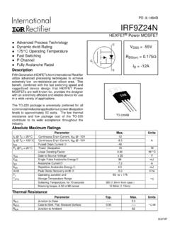
Transcription of INSULATED GATE BIPOLAR TRANSISTOR
1 IRG7CH81K10EF-R VCES = 1200V IC(Nominal) = 150A TJ(max) = 175 C VCE(on) typ = @ IC= 150A Applications Medium Power Drives UPS HEV Inverter Welding ECGn-channel Base part number Package Type Standard Pack Orderable part number Form Quantity IRG7CH81K10EF-R Die on Film Wafer 1 IRG7CH81K10EF-R Mechanical Parameter Die Size x mm2 Minimum Street Width 75 m Emiter Pad Size (Included gate Pad) See Die Drawing mm2 gate Pad Size x Area Total / Active / Thickness 140 m Wafer Size 200 mm Notch Position 0 Degrees Maximum-Possible Chips per Wafer 164 pcs.
2 Passivation Front side Silicon Nitride Front Metal Al, Si (4 m) Backside Metal Al - Ti - Ni - Ag (1kA - 1kA - 4kA - 6kA ) Die Bond Electrically conductive epoxy or solder Reject Ink Dot Size mm diameter minimum G C E gate Collector Emitter INSULATED gate BIPOLAR TRANSISTOR Features Benefits Low VCE(ON) and switching Losses High efficiency in a wide range of applications and switching frequencies Square RBSOA and Maximum Junction Temperature 175 C Improved Reliability due to rugged hard switching performance and higher power capability Positive VCE (ON) Temperature Coefficient Excellent current sharing in parallel operation Integrated gate Resistor Easier Paralleling with Integrated gate Resistor 1 2013 International Rectifier Submit Datasheet Feedback November 22, 2013 IRG7CH81K10EF-R 2 2013 International Rectifier Submit Datasheet Feedback November 22, 2013 Static Characteristics (Tested on wafers) @ TJ=25 C Parameter Min.
3 Typ. Max. Units Conditions V(BR)CES Collector-to-Emitter Breakdown Voltage 1200 VGE = 0V, IC = 250 A VCE(sat) Collector-to-Emitter Saturated Voltage VGE = 15V, IC = 150A, TJ = 25 C VGE(th) gate -Emitter Threshold Voltage IC = , VGE = VCE ICES Zero gate Voltage Collector Current 25 A VCE = 1200V, VGE = 0V IGES gate Emitter Leakage Current 400 nA VCE = 0V, VGE = 30V RG INTERNAL Internal gate Resistance Electrical Characteristics (Not subject to production test-Verified by design/characterization) Parameter Min.
4 Typ. Max. Units Conditions VCE(sat) Collector-to-Emitter Saturated Voltage V VGE = 15V, IC = 150A , TJ = 25 C VGE = 15V, IC = 150A , TJ = 150 C SCSOA Short Circuit Safe Operating Area 10 s VGE=15V, VCC=600V RG=5 , VP =1200V,TJ 150 C RBSOA Reverse Bias Safe Operating Area FULL SQUARE TJ = 175 C, IC = 600A VCC = 960V, Vp 1200V Rg = 5 , VGE = +20V to 0V Ciss Input Capacitance 15330 pF VGE = 0V Coss Output Capacitance 670 VCE = 30V Crss Reverse Transfer Capacitance 390 = Qg Total gate Charge (turn-on)
5 745 nC IC = 150A Qge gate -to-Emitter Charge (turn-on) 190 VGE = 15V Qgc gate -to-Collector Charge (turn-on) 365 VCC = 600V Switching Characteristics (Inductive Load-Not subject to production test-Verified by design/characterization) Parameter Min. Typ. Max. Units Conditions td(on) Turn-On delay time 70 ns IC = 150A, VCC = 600V tr Rise time 130 RG = , VGE=15V, L=100 H td(off) Turn-Off delay time 330 TJ = 25 C tf Fall time 70 td(on) Turn-On delay time 70 IC = 150A, VCC = 600V tr Rise time 140 RG = , VGE=15V, L= 100 H td(off) Turn-Off delay time 450 TJ = 175 C tf Fall time 110 V Notes: The current in the application is limited by TJMax and the thermal properties of the assembly.
6 Not subject to production test- Verified by design / characterization. Values influenced by parasitic L and C in measurement. VCC = 80% (VCES), VGE = 20V, L = H, RG = 5 . Die level characterization. Pulse width 400 s; duty cycle 2%. Parameter Max. Units VCE Collector-Emitter Voltage, TJ=25 C 1200 V IC DC Collector Current A ILM Clamped Inductive Load Current 600 A VGE gate Emitter Voltage 30 V TJ.
7 TSTG Operating Junction and Storage Temperature -40 to +175 C Maximum Ratings IRG7CH81K10EF-R 3 2013 International Rectifier Submit Datasheet Feedback November 22, 2013 Die Drawing [.0394] [.4877] [.4877] [.0673] [.1330] [.4205] [.1314]Internal gate Resistance Test X [.0069 ] [.0317]4. DIE THICKNESS = [ .0055]1. ALL DIMENSIONS ARE SHOWN IN MILLIMETERS [ INCHES] .2. CONTROLLING DIMENSION: INCHESNOTES:3. DIE WIDTH AND LENGTH TOLERANCE: [.002] IRG7CH81K10EF-R 4 2013 International Rectifier Submit Datasheet Feedback November 22, 2013 Additional Testing and Screening For Customers requiring product supplied as Known Good Die (KGD) or requiring specific die level testing, please con-tact your local IR Sales.
8 Shipping Sawn Wafer on Film. Please contact your local IR sales office for non standard shipping options Handling Product must be handled only at ESD safe workstations. Standard ESD precautions and safe work environ-ments are as defined in MIL-HDBK-263. Product must be handled only in a class 10,000 or better-designated clean room environment. Singulated die are not to be handled with tweezers. A vacuum wand with a non-metallic ESD protected tip should be used. Wafer/Die Storage Proper storage conditions are necessary to prevent product contamination and/or degradation after shipment.
9 Note: To reduce the risk of contamination or degradation, it is recommended that product not being used in the assembly process be returned to their original containers and resealed with a vacuum seal process. Sawn wafers on a film frame are intended for immediate use and have a limited shelf life. Further Information For further information please contact your local IR Sales office or email your enquiry to . IR WORLD HEADQUARTERS: 101 N. Sepulveda Blvd., El Segundo, California 90245, USA To contact International Rectifier, please visit