Transcription of Lecture 3 - Data Converters
1 Colorado State University Dept of Electrical and Computer EngineeringECE423 1 / 30 Lecture 3 - data ConvertersJames Barnes 2014 Lab2 InfoLab2 Info Lissajou Figures Support Files UpdateIntroduction to ADCsQuantization Noise andEffective Number of BitsOversampling ADCN oise Filtering andDecimationColorado State University Dept of Electrical and Computer EngineeringECE423 2 / 30 Lissajou FiguresColorado State University Dept of Electrical and Computer EngineeringECE423 3 / 30 Lissajou figures: a way of combining two phasors. Plot x-component of onephasor on x axis and x-component of other phasor on y-axis. Ref: Files UpdateColorado State University Dept of Electrical and Computer EngineeringECE423 4 / 30 Minor tweaks to three support files to Fix compile problem when usinginput_sample() Increase heap size to copy and replace the eight support files used in to ADCsLab2 InfoIntroduction to ADCs References Classes of ADCs ADC Families Example.
2 Flash ADCQ uantization Noise andEffective Number of BitsOversampling ADCN oise Filtering andDecimationColorado State University Dept of Electrical and Computer EngineeringECE423 5 / 30 ReferencesColorado State University Dept of Electrical and Computer EngineeringECE423 6 / 30[1] David Jarman, A Brief Introduction to Sigma Delta Conversion , IntersilApplication Note AN9504, May [2] Sangil Park, Principles of Sigma-Delta Modulation forAnalog-to-DigitalConverters , Motorola [3] Demystifying Delta-Sigma ADCs , Maxim Application Note 1870, 2003 of ADCsColorado State University Dept of Electrical and Computer EngineeringECE423 7 / 30We can divide ADCs into classes as follows:1. Full Resolution Quantization(a) Nyquist rate sampling. The first designs. Still used in applicationswhich can afford the cost and power.
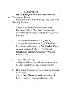
3 (b) Oversampling - can increase effective resolution but atthe cost ofpower and expense. For applications where ultimate performance Coarse Quantization - uses oversampling to increase the effective number ofbits. Newer technology, enabled by VLSI FamiliesColorado State University Dept of Electrical and Computer EngineeringECE423 8 / 30 Parallel processing => higher conversion rate Because hardware is expensive (chip cost, power), there is aspeed-accuracy : Flash ADCC olorado State University Dept of Electrical and Computer EngineeringECE423 9 / 30 Conversion consists of (1) sampling, (2) slicing, and (3) encoding. Questions: Where is the sampler in this diagram? Why the 3-input OR gates?Quantization Noise and Effective Numberof BitsLab2 InfoIntroduction to ADCsQuantization Noise andEffective Number of Bits Quantization as aWhite Noise Source Quantization NoisePower Signal-to-Noise Ratioand Effective Number ofBits of an ADCO versampling ADCN oise Filtering andDecimationColorado State University Dept of Electrical and Computer EngineeringECE423 10 / 30 Quantization as a White Noise SourceColorado State University Dept of Electrical and Computer EngineeringECE423 11 / 30 Consider quantization by a Nyquist-rate ADC with a can be modelled as introducing additive whitenoise distributed overa range 2to 2.
4 Where is the quantization level spacing and B is the numberof Noise PowerColorado State University Dept of Electrical and Computer EngineeringECE423 12 / 30 The total quantization noise power (variance) is< e2>=1 /2 /2e2qdeq=e3q3 /2eq= /2= xmin, the total noise powerNand noise power densityN(f)over the frequency range[ Fs/2, Fs/2]are given byN=x2r 2 2B12andN(f) =x2r 2 Ratio and Effective Numberof Bits of an ADCC olorado State University Dept of Electrical and Computer EngineeringECE423 13 / 30 The signal-to-noise ratio for a known input, commonly a sinewave, can be usedto determine the effective number of bits of a quantizer. Themeasured ENOBmay be less than the design specification because of other noise SNR is given bySN R(db) = 10log10(< signal power > < noise power >)For a full range sine wavex(t) =xr/2 sin(2 f t), the signal power is< x2>=x2r/8.
5 ThereforeSN R(db) = 10log10(32 22B) = + (1)andEN OB=SN R(db) (2)Studies have cast doubt on the accuracy of this formula because of unmodelledeffects, but it does show that the SNR doubles for every bit added to thequantizer, as ADCLab2 InfoIntroduction to ADCsQuantization Noise andEffective Number of BitsOversampling ADC Oversampling FullResolution ADC Reduced ResolutionOversamplingConverters Delta-SigmaPredecessor - DeltaModulator Frequency DomainAnalysis of DM Possible CircuitImplementations ofIntegrator Delta-Sigma converter Matlab Example - xvsxs Second OrderDelta-Sigma Modulator Frequency Responsein Z DomainNoise Filtering andDecimationColorado State University Dept of Electrical and Computer EngineeringECE423 14 / 30 Oversampling Full Resolution ADCC olorado State University Dept of Electrical and Computer EngineeringECE423 15 / 30A design challenge for Full Resolution Nyquist Rate sampling is theanti-aliasingfilter(AAF).
6 Oversampling can simplify the design of the AAF and also improvenoise performance because the total noise power remains thesame but isspread over a wider frequency the AAF can now have a very small flat region, it can be implementedwith a simple RC low pass total noise is still 212but theinband noise(dark region) is reduced to 212 OSR, whereOSRis the oversampling simple comb filter decimator, which performs a moving average, can recoverlog2(N)additional bits which can be appended to the physical wordlength of Resolution OversamplingConvertersColorado State University Dept of Electrical and Computer EngineeringECE423 16 / 30 Sampling at a rate higher than the input signal bandwidth: the signal change per sample time will small compared to the total range ofthe signal a lower resolution (# of bits) converter can be used.
7 But the quantizer should in some sense operate on thechangein the signalsince the last sample. The quantizer should utilize past values of the signal to predict the current value and the difference between the actual andpredicted value to correct the Predecessor - Delta ModulatorColorado State University Dept of Electrical and Computer EngineeringECE423 17 / 30 AKA predictive signal quantizer or delta modulation (DM). First used in telephony. Integrating path subtracts off the average value computed from past samples, adjustingthreshold of slicer Problems: Slope Overload , Granularity . Increasing integrating path gain A helps the firstproblem but hurts the Domain Analysis of DMColorado State University Dept of Electrical and Computer EngineeringECE423 18 / 30 Possible Circuit Implementations ofIntegratorColorado State University Dept of Electrical and Computer EngineeringECE423 19 / 30 These conceptual: there are a lot of practical details to be ConverterColorado State University Dept of Electrical and Computer EngineeringECE423 20 / 30 Move Integrator in front of shaping: Signal transfer function is a lowpass filter Noise transfer function is highpass filter Noise is pushed out of signal band!
8 Attenuated by following Example - xvsxsColorado State University Dept of Electrical and Computer EngineeringECE423 21 / 30 OSR=256, A= Order Delta-Sigma ModulatorColorado State University Dept of Electrical and Computer EngineeringECE423 22 / 30 Higher-order loops can be created by cascading integrators. The order=number of integrators in [1]Frequency Response in Z DomainColorado State University Dept of Electrical and Computer EngineeringECE423 23 / 30 There are two ways the first order loop is drawn. They give different results forthesignal transfer functionbut same result and implication for thenoisetransfer function. The analysis is as follows (whiteboard):Noise Filtering and DecimationLab2 InfoIntroduction to ADCsQuantization Noise andEffective Number of BitsOversampling ADCN oise Filtering andDecimation Delta-Sigma Signaland Noise Spectra SNR (and ENOB) vsOSR for Delta-SigmaModulators Decimation andFiltering Comb Filter Comb Filter asDecimator Final Operation - FIRF ilterColorado State University Dept of Electrical and Computer EngineeringECE423 24 / 30 Delta-Sigma Signal and Noise SpectraColorado State University Dept of Electrical and Computer EngineeringECE423 25 / 30 Digital low-pass filter removes most of quantization noise while preserving signalspectrumRef[3]SNR (and ENOB)
9 Vs OSR for Delta-SigmaModulatorsColorado State University Dept of Electrical and Computer EngineeringECE423 26 / 30 Ref[3]ENOB formula given earlier 16 bit resolution requiresSN Rof98dBDecimation and FilteringColorado State University Dept of Electrical and Computer EngineeringECE423 27 / 30 This is one way of doing decimation and filtering (the Motorola way).The comb filter sums the number of 1s in consecutive samples, irrespective oftheir locations in the sequence, essentially doing a movingaverage over thelength of the [2], Section 7 has a very nice description of the whole FilterColorado State University Dept of Electrical and Computer EngineeringECE423 28 / 30 The comb filter looks like this (example for N=4):Ref[2]Comb Filter as DecimatorColorado State University Dept of Electrical and Computer EngineeringECE423 29 / 30 The filter operation can be considered as anintegration-decimation-differentiation processRef[2]Final Operation - FIR FilterColorado State University Dept of Electrical and Computer EngineeringECE423 30 / 30 The comb filter does not have enough suppression of the out-of-band quantization noise has less than flat response in the basebandTherefore, the final FIR filter must boost the low-frequency response whileproviding additional suppression of out-of-band quantization [2]