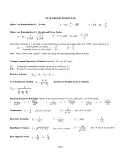
Transcription of LM1875 20W Audio Power Amplifier datasheet (Rev. A)
1 LM1875 . SNAS524A MAY 2004 REVISED MAY 2004. LM1875 20W Audio Power Amplifier Check for Samples: LM1875 . 1 FEATURES DESCRIPTION.. 2 Up to 30 Watts Output Power The LM1875 is a monolithic Power Amplifier offering very low distortion and high quality performance for AVO Typically 90 dB consumer Audio applications. Low Distortion: , 1 kHz, 20 W. The LM1875 delivers 20 watts into a 4 or 8 load Wide Power Bandwidth: 70 kHz on 25V supplies. Using an 8 load and 30V. Protection for AC and DC Short Circuits to supplies, over 30 watts of Power may be delivered. Ground The Amplifier is designed to operate with a minimum Thermal Protection with Parole circuit of external components. Device overload protection consists of both internal current limit and thermal High Current Capability: 4A shutdown. Wide Supply Range 16V-60V. The LM1875 design takes advantage of advanced Internal Output Protection Diodes circuit techniques and processing to achieve 94 dB Ripple Rejection extremely low distortion levels even at high output Plastic Power Package TO-220 Power levels.
2 Other outstanding features include high gain, fast slew rate and a wide Power bandwidth, large output voltage swing, high current capability, APPLICATIONS and a very wide supply range. The Amplifier is High Performance Audio Systems internally compensated and stable for gains of 10 or Bridge Amplifiers greater. Stereo Phonographs Servo Amplifiers Instrument Systems Connection Diagram Figure 1. NDH0005D, KC0005A, NEB0005E, NEB0005B, Front View 1. Please be aware that an important notice concerning availability, standard warranty, and use in critical applications of Texas Instruments semiconductor products and disclaimers thereto appears at the end of this data sheet. 2 All trademarks are the property of their respective owners. PRODUCTION DATA information is current as of publication date. Copyright 2004, Texas Instruments Incorporated Products conform to specifications per the terms of the Texas Instruments standard warranty.
3 Production processing does not necessarily include testing of all parameters. LM1875 . SNAS524A MAY 2004 REVISED MAY 2004 Typical Applications These devices have limited built-in ESD protection. The leads should be shorted together or the device placed in conductive foam during storage or handling to prevent electrostatic damage to the MOS gates. Absolute Maximum Ratings (1). Supply Voltage 60V. Input Voltage VEE to VCC. Storage Temperature 65 C to + 150 C. Junction Temperature 150 C. (Soldering, 10 seconds) 260 C. Lead Temperature JC 3 C. JA 73 C. (1) Absolute Maximum Ratings indicate limits beyond which damage to the device may occur. Operating Ratings indicate conditions for which the device is functional, but do not ensure specific performance limits. 2 Submit Documentation Feedback Copyright 2004, Texas Instruments Incorporated Product Folder Links: LM1875 . LM1875 .
4 SNAS524A MAY 2004 REVISED MAY 2004. Electrical Characteristics VCC=+25V, VEE= 25V, TAMBIENT=25 C, RL=8 , AV=20 (26 dB), fo=1 kHz, unless otherwise specified. Parameter Conditions Typical Tested Limits Units Supply Current POUT=0W 70 100 mA. Output Power (1) THD=1% 25 W. THD (1) POUT=20W, fo=1 kHz %. POUT=20W, fo=20 kHz %. POUT=20W, RL=4 , fo=1 kHz %. POUT=20W, RL=4 , fo=20 kHz %. Offset Voltage 1 15 mV. Input Bias Current 2 A. Input Offset Current 0 A. Gain-Bandwidth Product fo=20 kHz MHz Open Loop Gain DC 90 dB. PSRR VCC, 1 kHz, 1 Vrms 95 52 dB. VEE, 1 kHz, 1 Vrms 83 52 dB. Max Slew Rate 20W, 8 , 70 kHz BW 8 V/ s Current Limit VOUT = VSUPPLY 10V 4 3 A. Equivalent Input Noise Voltage RS=600 , CCIR 3 Vrms (1) Assumes the use of a heat sink having a thermal resistance of 1 C/W and no insulator with an ambient temperature of 25 C. Because the output limiting circuitry has a negative temperature coefficient, the maximum output Power delivered to a 4 load may be slightly reduced when the tab temperature exceeds 55 C.
5 Typical Applications For Single Supply Operation Figure 2. Copyright 2004, Texas Instruments Incorporated Submit Documentation Feedback 3. Product Folder Links: LM1875 . LM1875 . SNAS524A MAY 2004 REVISED MAY 2004 Typical Performance Characteristics THD vs Power Output THD vs Frequency Figure 3. Figure 4. Power Output vs Supply Supply Current vs Supply Voltage Voltage Figure 5. Figure 6. PSRR vs Frequency Device Dissipation vs Ambient Temperature . INTERFACE = 1 C/W. See Application Hints. Figure 7. Figure 8. 4 Submit Documentation Feedback Copyright 2004, Texas Instruments Incorporated Product Folder Links: LM1875 . LM1875 . SNAS524A MAY 2004 REVISED MAY 2004. Typical Performance Characteristics (continued). Power Dissipation vs Power Output Power Dissipation vs Power Output Figure 9. Figure 10. IOUT vs VOUT-Current Limit/. Safe Operating Area Boundary Open Loop Gain and Phase vs Frequency Thermal shutdown with infinite heat sink Thermal shutdown with 1 C/W heat sink Figure 11.
6 Figure 12. Input Bias Current vs Supply Voltage Figure 13. Copyright 2004, Texas Instruments Incorporated Submit Documentation Feedback 5. Product Folder Links: LM1875 . LM1875 . SNAS524A MAY 2004 REVISED MAY 2004 Schematic Diagram 6 Submit Documentation Feedback Copyright 2004, Texas Instruments Incorporated Product Folder Links: LM1875 . LM1875 . SNAS524A MAY 2004 REVISED MAY 2004. APPLICATION HINTS. STABILITY. The LM1875 is designed to be stable when operated at a closed-loop gain of 10 or greater, but, as with any other high-current Amplifier , the LM1875 can be made to oscillate under certain conditions. These usually involve printed circuit board layout or output/input coupling. Proper layout of the printed circuit board is very important. While the LM1875 will be stable when installed in a board similar to the ones shown in this data sheet, it is sometimes necessary to modify the layout somewhat to suit the physical requirements of a particular application.
7 When designing a different layout, it is important to return the load ground, the output compensation ground, and the low level (feedback and input) grounds to the circuit board ground point through separate paths. Otherwise, large currents flowing along a ground conductor will generate voltages on the conductor which can effectively act as signals at the input, resulting in high frequency oscillation or excessive distortion. It is advisable to keep the output compensation components and the F supply decoupling capacitors as close as possible to the LM1875 to reduce the effects of PCB trace resistance and inductance. For the same reason, the ground return paths for these components should be as short as possible. Occasionally, current in the output leads (which function as antennas) can be coupled through the air to the Amplifier input, resulting in high-frequency oscillation.
8 This normally happens when the source impedance is high or the input leads are long. The problem can be eliminated by placing a small capacitor (on the order of 50 pF to 500 pF) across the circuit input. Most Power amplifiers do not drive highly capacitive loads well, and the LM1875 is no exception. If the output of the LM1875 is connected directly to a capacitor with no series resistance, the square wave response will exhibit ringing if the capacitance is greater than about F. The Amplifier can typically drive load capacitances up to 2. F or so without oscillating, but this is not recommended. If highly capacitive loads are expected, a resistor (at least 1 ) should be placed in series with the output of the LM1875 . A method commonly employed to protect amplifiers from low impedances at high frequencies is to couple to the load through a 10 resistor in parallel with a 5 H inductor.
9 DISTORTION. The preceding suggestions regarding circuit board grounding techniques will also help to prevent excessive distortion levels in Audio applications. For low THD, it is also necessary to keep the Power supply traces and wires separated from the traces and wires connected to the inputs of the LM1875 . This prevents the Power supply currents, which are large and nonlinear, from inductively coupling to the LM1875 inputs. Power supply wires should be twisted together and separated from the circuit board. Where these wires are soldered to the board, they should be perpendicular to the plane of the board at least to a distance of a couple of inches. With a proper physical layout, THD levels at 20 kHz with 10W output to an 8 load should be less than , and less than at 1 kHz. CURRENT LIMIT AND SAFE OPERATING AREA (SOA) PROTECTION. A Power Amplifier 's output transistors can be damaged by excessive applied voltage, current flow, or Power dissipation.
10 The voltage applied to the Amplifier is limited by the design of the external Power supply, while the maximum current passed by the output devices is usually limited by internal circuitry to some fixed value. Short- term Power dissipation is usually not limited in monolithic Audio Power amplifiers, and this can be a problem when driving reactive loads, which may draw large currents while high voltages appear on the output transistors. The LM1875 not only limits current to around 4A, but also reduces the value of the limit current when an output transistor has a high voltage across it. When driving nonlinear reactive loads such as motors or loudspeakers with built-in protection relays, there is a possibility that an Amplifier output will be connected to a load whose terminal voltage may attempt to swing beyond the Power supply voltages applied to the Amplifier . This can cause degradation of the output transistors or catastrophic failure of the whole circuit .