Transcription of Low Voltage, 1.15 V to 5.5 V, 4-Channel, …
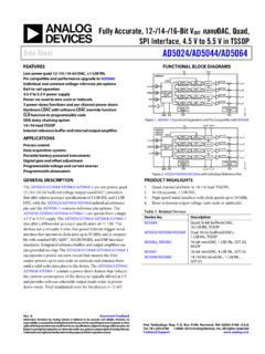
1 Low Voltage, V to V, 4- channel , bidirectional logic Level translator data Sheet ADG3304. FEATURES FUNCTIONAL BLOCK DIAGRAM. bidirectional level translation VCCA VCCY. Operates from V to V. Low quiescent current < 5 A A1 Y1. No direction pin Qualified for automotive applications A2 Y2. APPLICATIONS A3 Y3. SPI, MICROWIRE level translation Low voltage ASIC level translation A4 Y4. Smart card readers Cell phones and cell phone cradles EN. Portable communications devices 04860-001. Telecommunications equipment GND. Network switches and routers Figure 1. Storage systems (SAN/NAS). Computing/server applications GPS. Portable POS systems Low cost serial interfaces GENERAL DESCRIPTION. The ADG3304 is a bidirectional logic level translator that con- The enable pin (EN) provides three-state operation on both the tains four bidirectional channels.
2 It can be used in multivoltage A side and the Y side pins. When the EN pin is pulled low, the digital system applications, such as data transfer, between a low terminals on both sides of the device are in the high impedance voltage digital signal processing controller and a higher voltage state. The EN pin is referred to the VCCA supply voltage and device using SPI and MICROWIRE interfaces. The internal driven high for normal operation. architecture allows the device to perform bidirectional logic level translation without an additional signal to set the direction The ADG3304 is available in compact 14-lead TSSOP, 12-ball in which the translation takes place. WLCSP, and 20-lead LFCSP. It is guaranteed to operate over the V to V supply voltage range. The voltage applied to VCCA sets the logic levels on the A side of PRODUCT HIGHLIGHTS.
3 The device, while VCCY sets the levels on the Y side. For proper operation, VCCA must always be less than VCCY. The VCCA-com- 1. bidirectional level translation. patible logic signals applied to the A side of the device appear as 2. Fully guaranteed over the V to V supply range. VCCY-compatible levels on the Y side. Similarly, VCCY-compatible 3. No direction pin. logic levels applied to the Y side of the device appear as VCCA- 4. Available in 14-lead TSSOP, 12-ball WLCSP, and 20-lead compatible logic levels on the A side. LFCSP. Rev. E Document Feedback Information furnished by analog devices is believed to be accurate and reliable. However, no responsibility is assumed by analog devices for its use, nor for any infringements of patents or other rights of third parties that may result from its use.
4 Specifications subject to change without notice. No One Technology Way, Box 9106, Norwood, MA 02062-9106, license is granted by implication or otherwise under any patent or patent rights of analog devices . Tel: 2005 2016 analog devices , Inc. All rights reserved. Trademarks and registered trademarks are the property of their respective owners. Technical Support ADG3304 data Sheet TABLE OF CONTENTS. Features .. 1 Theory of Operation .. 17. Applications .. 1 Level translator Architecture .. 17. Functional Block Diagram .. 1 Input Driving Requirements .. 17. General Description .. 1 Output Load Requirements .. 17. Product Highlights .. 1 Enable Operation .. 17. Revision History .. 2 Power Supplies .. 17. 3 data Rate .. 18. Absolute Maximum 6 19. ESD Caution .. 6 Layout 19. Pin Configurations and Function Descriptions.
5 7 Outline Dimensions .. 20. Typical Performance Characteristics .. 9 Ordering Guide .. 21. Test Circuits .. 13 Automotive Products .. 21. Terminology .. 16. REVISION HISTORY. 4/16 Rev. D to Rev. E 12/05 Rev. A to Rev. B. Changed CP-20-1 to CP-20-6 .. Throughout Changes to Table Changes to Figure 3 and Table 3 .. 7 Changes to Table Moved Figure 4 .. 8 Changes to Figure 3 and Table 4 ..7. Updated Outline Dimensions .. 21 Updated Outline Dimensions .. 19. Changes to Ordering Guide .. 21 Changes to Ordering Guide .. 21. 4/13 Rev. C to Rev. D 6/05 Rev. 0 to Rev. A. Changes to Figure 3 and Table 4 .. 7 Added LFCSP Package .. Universal 12/12 Rev. B to Rev. C 1/05 Revision 0: Initial Version Changes to Table 1 .. 3. Changes to Table 2 .. 6. Changes to VCCY Description, Table 3 and Table 4.
6 7. Changes to Ordering Guide .. 20. Added Automotive Products Section .. 20. Rev. E | Page 2 of 21. data Sheet ADG3304. SPECIFICATIONS. VCCY = V to V, VCCA = V to VCCY, GND = 0 V, TA = 25 C. All specifications TMIN to TMAX, unless otherwise noted. Table 1. B Version 1. Parameter Symbol Test Conditions/Comments Min Typ Max Unit logic INPUTS/OUTPUTS. A Side Input High Voltage 2 VIHA VCCA = V + V/ V VCCA V. VCCA = V V VCCA V. VCCA = V V V. VCCA = V V V. VCCA = 5 V V VCCA V. Input Low Voltage2 VILA VCCA = V + V/ V VCCA V. VCCA = V V VCCA V. VCCA = V V V. VCCA = V V V. VCCA = 5 V V VCCA V. Output High Voltage VOHA VY = VCCY, IOH = 20 A, see Figure 29 VCCA V. Output Low Voltage VOLA VY = 0 V, IOL = 20 A, see Figure 29 V. Capacitance2 CA f = 1 MHz, EN = 0, see Figure 34 9 pF. Leakage Current ILA, Hi-Z VA = 0 V/VCCA, EN = 0, see Figure 31 1 A.
7 Y Side Input High Voltage2 VIHY VCCY = V V VCCY V. VCCY = V V V. VCCY = V V 2 V. VCCY = 5 V V VCCY V. Input Low Voltage2 VILY VCCY = V V VCCY V. VCCY = V V V. VCCY = V V V. VCCY = 5 V V VCCY V. Output High Voltage VOHY VA = VCCA, IOH = 20 A, see Figure 30 VCCY V. Output Low Voltage VOLY VA = 0 V, IOL = 20 A, see Figure 30 V. Capacitance2 CY f = 1 MHz, EN = 0, see Figure 35 6 pF. Leakage Current ILY, Hi-Z VY = 0 V/VCCY, EN = 0, see Figure 32 1 A. Enable (EN). Input High Voltage2 VIHEN VCCA = V + V/ V VCCA V. VCCA = V V VCCA V. VCCA = V V V. VCCA = V V V. VCCA = 5 V V VCCA V. Input Low Voltage2 VILEN VCCA = V + V/ V VCCA V. VCCA = V V VCCA V. VCCA = V V V. VCCA = V V V. VCCA = 5 V V VCCA V. Leakage Current ILEN VEN = 0 V/VCCA, VA = 0 V, see Figure 33 1 A. Capacitance2 CEN 3 pF. Enable Time2 tEN RS = RT = 50 , VA = 0 V/VCCA (A Y), 1 s VY = 0 V/VCCY (Y A), see Figure 36.
8 Rev. E | Page 3 of 21. ADG3304 data Sheet B Version 1. Parameter Symbol Test Conditions/Comments Min Typ Max Unit SWITCHING CHARACTERISTICS2. V V VCCA VCCY, VCCY = 5 V V. A Y Level Translation RS = RT = 50 , CL = 50 pF, see Figure 37. Propagation Delay tP, A Y 6 10 ns Rise Time tR, A Y 2 ns Fall Time tF, A Y 2 ns Maximum data Rate DMAX, A Y 50 Mbps channel -to- channel Skew tSKEW, A Y 2 4 ns Part-to-Part Skew tPPSKEW, A Y 3 ns Y A Level Translation RS = RT = 50 , CL = 15 pF, see Figure 38. Propagation Delay tP, Y A 4 7 ns Rise Time tR, Y A 1 3 ns Fall Time tF, Y A 3 7 ns Maximum data Rate DMAX, Y A 50 Mbps channel -to- channel Skew tSKEW, Y A 2 ns Part-to-Part Skew tPPSKEW, Y A 2 ns V V VCCA VCCY, VCCY = V V. A Y Translation RS = RT = 50 , CL = 50 pF, see Figure 37. Propagation Delay tP, A Y 8 11 ns Rise Time tR, A Y 2 5 ns Fall Time tF, A Y 2 5 ns Maximum data Rate DMAX, A Y 50 Mbps channel -to- channel Skew tSKEW, A Y 2 4 ns Part-to-Part Skew tPPSKEW, A Y 4 ns Y A Translation RS = RT = 50 , CL = 15 pF, see Figure 38.
9 Propagation Delay tP, Y A 5 8 ns Rise Time tR, Y A 2 ns Fall Time tF, Y A 2 ns Maximum data Rate DMAX, Y A 50 Mbps channel -to- channel Skew tSKEW, Y A 2 3 ns Part-to-Part Skew tPPSKEW, Y A 3 ns V to V VCCA VCCY, VCCY = V V. A Y Translation RS = RT = 50 , CL = 50 pF, see Figure 37. Propagation Delay tP, A Y 9 18 ns Rise Time tR, A Y 3 5 ns Fall Time tF, A Y 2 5 ns Maximum data Rate DMAX, A Y 40 Mbps channel -to- channel Skew tSKEW, A Y 2 5 ns Part-to-Part Skew tPPSKEW, A Y 10 ns Y A Translation RS = RT = 50 , CL = 15 pF, see Figure 38. Propagation Delay tP, Y A 5 9 ns Rise Time tR, Y A 2 4 ns Fall Time tF, Y A 2 4 ns Maximum data Rate DMAX, Y A 40 Mbps channel -to- channel Skew tSKEW, Y A 2 4 ns Part-to-Part Skew tPPSKEW, Y A 4 ns Rev. E | Page 4 of 21. data Sheet ADG3304. B Version 1. Parameter Symbol Test Conditions/Comments Min Typ Max Unit V to V VCCA VCCY, VCCY = V V.
10 A Y Translation RS = RT = 50 , CL = 50 pF, see Figure 37. Propagation Delay tP, A Y 12 25 ns Rise Time tR, A Y 7 12 ns Fall Time tF, A Y 3 5 ns Maximum data Rate DMAX, A Y 25 Mbps channel -to- channel Skew tSKEW, A Y 2 5 ns Part-to-Part Skew tPPSKEW, A Y 15 ns Y A Translation RS = RT = 50 , CL = 15 pF, see Figure 38. Propagation Delay tP, Y A 14 35 ns Rise Time tR, Y A 5 16 ns Fall Time tF, Y A ns Maximum data Rate DMAX, Y A 25 Mbps channel -to- channel Skew tSKEW, Y A 3 ns Part-to-Part Skew tPPSKEW, Y A ns V V VCCA VCCY, VCCY = V V. A Y Translation RS = RT = 50 , CL = 50 pF, see Figure 37. Propagation Delay tP, A Y 7 10 ns Rise Time tR, A Y 4 ns Fall Time tF, A Y 2 5 ns Maximum data Rate DMAX, A Y 60 Mbps channel -to- channel Skew tSKEW, A Y 2 ns Part-to-Part Skew tPPSKEW, A Y 4 ns Y A Translation RS = RT = 50 , CL = 15 pF, see Figure 38.