Transcription of LT8301 (Rev. B) - Analog Devices
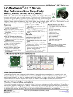
1 LT83011 Rev. BFor more information FeedbackTYPICAL APPLICATION FEATURESDESCRIPTION42 VIN Micropower No-Opto Isolated Flyback Converter with 65 SwitchThe LT 8301 is a micropower isolated flyback converter. By sampling the isolated output voltage directly from the primary-side flyback waveform, the part requires no third winding or opto-isolator for regulation. The output voltage is programmed with a single external resistor. Internal compensation and soft-start further reduce external com-ponent count. Boundary mode operation provides a small magnetic solution with excellent load regulation. Low ripple Burst Mode operation maintains high efficiency at light load while minimizing the output voltage ripple . A , 65V DMOS power switch is integrated along with all high voltage circuitry and control logic into a 5-lead ThinSOT LT8301 operates from an input voltage range of to 42V and can deliver up to 6W of isolated output power.
2 The high level of integration and the use of boundary and low ripple burst modes result in a simple to use, low component count, and high efficiency application solution for isolated power delivery. All registered trademarks and trademarks are the property of their respective owners. Protected by Patents, including 5438499, 7463497, and to 36 VIN/5 VOUT Micropower Isolated Flyback ConverterAPPLICATIONS to 42V Input Voltage Range , 65V Internal DMOS Power Switch nLow Quiescent Current: n100 A in Sleep Mode n350 A in Active Mode nBoundary Mode Operation at Heavy Load nLow- ripple Burst Mode Operation at Light Load nMinimum Load < (Typ) of Full Output nVOUT Set with a Single External Resistor nNo Transformer Third Winding or Opto-Isolator Required for Regulation nAccurate EN/UVLO Threshold and Hysteresis nInternal Compensation and Soft-Start nOutput Short-Circuit Protection n5-Lead TSOT-23 Package nAEC-Q100 Qualified for Automotive Applications nIsolated Telecom, Automotive, Industrial, Medical Power Supplies nIsolated Auxiliary/Housekeeping Power SuppliesEfficiency vs Load CurrentLT83013.
3 1 RFBSW40 HEN/UVLO10 TO 36 VVOUT+5V6mA TO (VIN = 5V)6mA TO (VIN = 12V)6mA TO (VIN = 24V)6mA TO (VIN = 36V)VOUT GND154k 100 F8301 TA01aLOAD CURRENT (A)060 EFFICIENCY (%) = 5 VVIN = 12 VVIN = 24 VVIN = 36 VLT83012 Rev. BFor more information CONFIGURATIONABSOLUTE MAXIMUM RATINGSSW (Note 2) .. 65 VVIN .. 42 VEN/UVLO .. VINRFB .. VIN to VINC urrent into RFB .. 200 AOperating Junction Temperature Range (Notes 3, 4)LT8 301E, LT8 301I .. 40 C to 125 C LT8 301J, LT8 301H .. 40 C to 150 C LT8 301MP .. 55 C to 150 CStorage Temperature Range .. 65 C to 150 C (Note 1)EN/UVLO 1 GND 2 TOP VIEWS5 PACKAGE5-LEAD PLASTIC TSOT-23 JA = 150 C/WRFB 35 VIN4 SWORDER INFORMATIONLEAD FREE FINISHTAPE AND REELPART MARKING*PACKAGE DESCRIPTIONTEMPERATURE RANGELT8301ES5#TRMPBFLT8301ES5#TRPBFLTGM F5-Lead Plastic TSOT-23 40 C to 125 CLT8301IS5#TRMPBFLT8301IS5#TRPBFLTGMF5-L ead Plastic TSOT-23 40 C to 125 CLT8301JS5#TRMPBFLT8301JS5#TRPBFLTGMF5-L ead Plastic TSOT-23 40 C to 150 CLT8301HS5#TRMPBFLT8301HS5#TRPBFLTGMF5-L ead Plastic TSOT-23 40 C to 150 CLT8301 MPS5#TRMPBFLT8301 MPS5#TRPBFLTGMF5-Lead Plastic TSOT-23 55 C to 150 CAUTOMOTIVE PRODUCTS**LT8301ES5#WTRMPBFLT8301ES5#WTR PBFLTGMF5-Lead Plastic TSOT-23 40 C to 125 CLT8301IS5#WTRMPBFLT8301IS5#WTRPBFLTGMF5 -Lead Plastic TSOT-23 40 C to 125 CLT8301JS5#WTRMPBFLT8301JS5#WTRPBFLTGMF5 -Lead Plastic TSOT-23 40 C to 150 CLT8301HS5#WTRMPBFLT8301HS5#WTRPBFLTGMF5 -Lead Plastic
4 TSOT-23 40 C to 150 CContact the factory for parts specified with wider operating temperature ranges. *The temperature grade is identified by a label on the shipping and reel specifications. Some packages are available in 500 unit reels through designated sales channels with #TRMPBF suffix.**Versions of this part are available with controlled manufacturing to support the quality and reliability requirements of automotive applications. These models are designated with a #W suffix. Only the automotive grade products shown are available for use in automotive applications. Contact your local Analog Devices account representative for specific product ordering information and to obtain the specific Automotive Reliability reports for these BFor more information CHARACTERISTICSNote 1: Stresses beyond those listed under Absolute Maximum Ratings may cause permanent damage to the device.
5 Exposure to any Absolute Maximum Rating condition for extended periods may affect device reliability and 2: The SW pin is rated to 65V for transients. Depending on the leakage inductance voltage spike, operating waveforms of the SW pin should be derated to keep the flyback voltage spike below 65V as shown in Figure 3: The LT8301E is guaranteed to meet performance specifications from 0 C to 125 C operating junction temperature. Specifications over the 40 C to 125 C operating junction temperature range are assured by design, characterization and correlation with statistical process controls. The l denotes the specifications which apply over the full operating temperature range, otherwise specifications are at TA = 25 C.
6 VIN = 5V, VEN/UVLO = VIN unless otherwise Voltage UVLO ThresholdRising VIQVIN Quiescent CurrentVEN/UVLO = VEN/UVLO = Sleep Mode (Switch Off) Active Mode (Switch On) 215 100 3502 A A A AEN/UVLO Shutdown Threshold For Lowest Off Enable ThresholdFalling VIHYSEN/UVLO Hysteresis CurrentVEN/UVLO = VEN/UVLO = VEN/UVLO = A A AfMINM inimum Switching (MIN)Minimum Switch-On Time170nstOFF(MAX)Maximum Switch-Off TimeBackup Timer190 sISW(MAX)Maximum SW Current (MIN)Minimum SW Current (ON)Switch On-ResistanceISW = ILKGS witch Leakage CurrentVIN = 42V, VSW = AIRFBRFB Regulation ARFB Regulation Current Line VIN LT8301I is guaranteed over the full 40 C to 125 C operating junction temperature range. The LT8301J and LT8301H are guaranteed over the full 40 C to 150 C operating junction temperature range.
7 The LT8301MP is guaranteed over the full 55 C to 150 C operating junction temperature range. high junction temperatures degrade operating lifetimes. Operating lifetime is derated at junction temperature greater than 125 4: The LT8301 includes overtemperature protection that is intended to protect the device during momentary overload conditions. Junction temperature will exceed 150 C when overtemperature protection is active. Continuous operation above the specified maximum operating junction temperature may impair device BFor more information PERFORMANCE CHARACTERISTICSB oundary Mode WaveformsDiscontinuous Mode WaveformsBurst Mode WaveformsVIN Shutdown CurrentVIN Quiescent Current, Sleep ModeVIN Quiescent Current, Active ModeOutput Load and Line RegulationOutput Short-Circuit ProtectionSwitching Frequency vs Load CurrentTA = 25 C, unless otherwise CURRENT (A) FREQUENCY (kHz)VIN = 5 VVIN = 12 VVIN = 24 VVIN = 36 VFRONT PAGE APPLICATIONVIN (V)00IQ ( A)26810102025458301 G074515303540TJ = 150 CTJ = 25 CTJ = 55 CVIN (V)0IQ ( A)100110120408301 G0890806010203054515253570140130TJ = 150 CTJ = 25 CTJ = 55 CVIN (V)0IQ ( A)320340360408301 G09300280102030545152535400380TJ = 150 CTJ = 25 CTJ = 55 CLOAD CURRENT (A)0 OUTPUT VOLTAGE (V)
8 PAGE = 5 VVIN = 12 VVIN = 24 VVIN = 36 VLOAD CURRENT (A)00 OUTPUT VOLTAGE (V) = 5 VVIN = 12 VVIN = 24 VVIN = 36 VFRONT PAGE APPLICATIONVOUT50mV/DIVVSW20V/DIV5 s/DIVFRONT PAGE APPLICATIONVIN = 12 VILOAD = 600mA8301 G04 VOUT50mV/DIVVSW20V/DIV5 s/DIVFRONT PAGE APPLICATIONVIN = 12 VILOAD = 200mA8301 G05 VOUT50mV/DIVVSW20V/DIV20 s/DIVFRONT PAGE APPLICATIONVIN = 12 VILOAD = 6mA8301 G06LT83015 Rev. BFor more information PERFORMANCE CHARACTERISTICSRDS(ON)Switch Current LimitMaximum Switching FrequencyMinimum Switching FrequencyMinimum Switch-On TimeMinimum Switch-Off TimeEN/UVLO Enable ThresholdEN/UVLO Hysteresis CurrentRFB Regulation CurrentTA = 25 C, unless otherwise ( C)VEN/UVLO (V) G101507550125100250 25 50 TEMPERATURE ( C)IHYS ( A)5123408301 G111507550125100250 25 50 TEMPERATURE ( C)IRFB ( A)10510110210310410096979899958301 G121507550125100250 25 50 TEMPERATURE ( C)RESISTANCE (m )100020040060080008301 G131507550125100250 25 50 TEMPERATURE ( C) 50 ISW (A) CURRENT LIMITMINIMUM CURRENT LIMITTEMPERATURE ( C) 500 FREQUENCY (kHz)1002003004000501001508301 G15500600 252575125 TEMPERATURE ( C) 500 FREQUENCY (kHz)5101520 25025508301 G1675100125150 TEMPERATURE ( C)TIME (ns)
9 50010020030040008301 G171507550125100250 25 50 TEMPERATURE ( C)TIME (ns)50010020030040008301 G181507550125100250 25 50LT83016 Rev. BFor more information FUNCTIONSEN/UVLO (Pin 1): Enable/Undervoltage Lockout. The EN/UVLO pin is used to enable the LT8301 . Pull the pin below to shut down the LT8301 . This pin has an accurate threshold and can be used to program a VIN undervoltage lockout (UVLO) threshold using a resis-tor divider from VIN to ground. A A current hysteresis allows the programming of VIN UVLO hysteresis. If neither function is used, tie this pin directly to (Pin 2): Ground. Tie this pin directly to local ground (Pin 3): Input Pin for External Feedback Resistor. Connect a resistor from this pin to the transformer primary SW pin. The ratio of the RFB resistor to an internal 10k resistor, times a trimmed reference voltage, deter-mines the output voltage (plus the effect of any non-unity transformer turns ratio).
10 Minimize trace area at this (Pin 4): Drain of the 65V Internal DMOS Power Switch. Minimize trace area at this pin to reduce EMI and voltage (Pin 5): Input Supply. The VIN pin supplies current to internal circuitry and serves as a reference voltage for the feedback circuitry connected to the RFB pin. Locally bypass this pin to ground with a DIAGRAM8301 BD + +OSCILLATOR1 AM2M3 BOUNDARYDETECTORDRIVER +A2A3 RSENSEM1gmRREF10k AR2EN/UVLOM4345 + :1 DOUTLSECLPRIVOUT+VOUT COUTCINR1LT83017 Rev. BFor more information LT8301 is a current mode switching regulator IC designed specially for the isolated flyback topology. The key problem in isolated topologies is how to commu-nicate the output voltage information from the isolated secondary side of the transformer to the primary side for regulation.