Transcription of Adjustable Output, Positive D2PAK 3 D2T SUFFIX CASE 936
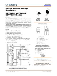
1 DATA Semiconductor Components Industries, LLC, 2016 August, 2021 Rev. 171 Publication Order Number:LM317/DVoltage Regulator Adjustable Output, ALM317, NCV317 The LM317 is an Adjustable 3 terminal Positive voltage regulatorcapable of supplying in excess of A over an output voltage range V to 37 V. This voltage regulator is exceptionally easy to use andrequires only two external resistors to set the output voltage. Further, itemploys internal current limiting, thermal shutdown and safe areacompensation, making it essentially blow out LM317 serves a wide variety of applications including local, oncard regulation. This device can also be used to make a programmableoutput regulator, or by connecting a fixed resistor between theadjustment and output, the LM317 can be used as a precision Output Current in Excess of A Output Adjustable between V and 37 V Internal Thermal Overload Protection Internal Short Circuit Current Limiting Constant with Temperature Output Transistor Safe Area Compensation Floating Operation for High Voltage Applications Eliminates Stocking many Fixed Voltages Available in Surface Mount D2PA K 3, and Standard 3 LeadTransistor Package NCV Prefix for Automotive and Other Applications RequiringUnique Site and Control Change Requirements; AEC Q100 Qualified and PPAP Capable These Devices are Pb Free, Halogen Free/BFR Free and are RoHSCompliantFigure 1.
2 Standard Application** Cin is required if regulator is located an appreciable distance from power supply filter.** CO is not needed for stability, however, it does improve transient IAdj is controlled to less than 100 mA, the error associated with this term isnegligible in most + V 1)R2R1 ) IAdj R2LM317 VinVoutR1240R2 AdjustIAdjCin* mF+CO** mFTO 220T SUFFIXCASE 221 ABPin 1. Adjust2. Vout3. VinD2 PAK 3D2T SUFFIXCASE 936 Heatsink surface (shown as terminal 4 in case outline drawing) is connected to Pin surface connected to Pin detailed ordering and shipping information in the packagedimensions section on page 10 of this data INFORMATIONSee general marking information in the device markingsection on page 10 of this data MARKING INFORMATIONLM317, RATINGSR atingSymbolValueUnitInput Output Voltage DifferentialVI VO to 40 VdcPower DissipationCase 221 ATA = +25 CPDI nternally LimitedWThermal Resistance, Junction to AmbientqJA65 C/WThermal Resistance, Junction to C/WCase 936 (D2 PAK 3)TA = +25 CPDI nternally LimitedWThermal Resistance, Junction to AmbientqJA70 C/WThermal Resistance, Junction to C/WOperating Junction Temperature RangeTJ 55 to +150 CStorage Temperature RangeTstg 65 to +150 CStresses exceeding those listed in the Maximum Ratings table may damage the device.
3 If any of these limits are exceeded, device functionalityshould not be assumed, damage may occur and reliability may be CHARACTERISTICS(VI VO = V; IO = A for D2T and T packages; TJ = Tlow to Thigh (Note 1); Imax and Pmax (Note 2); unless otherwise noted.)CharacteristicsFigureSymbolMinTyp MaxUnitLine Regulation (Note 3), TA = +25 C, V VI VO 40 V1 Regline Regulation (Note 3), TA = +25 C, 10 mA IO ImaxVO VVO V2 Regload VOThermal Regulation, TA = +25 C (Note 4), 20 ms Pulse Regtherm VO/WAdjustment Pin Current3 IAdj 50100mAAdjustment Pin Current Change, V VI VO 40 V,10 mA IL Imax, PD Pmax1, 2 DIAdj Voltage, V VI VO 40 V, 10 mA IO Imax, PD Regulation (Note 3), V VI VO 40 V1 Regline Regulation (Note 3), 10 mA IO ImaxVO VVO V2 Regload VOTemperature Stability (Tlow TJ Thigh)3TS % VOMinimum Load Current to Maintain Regulation (VI VO = 40 V)3 ILmin Output CurrentVI VO 15 V, PD Pmax, T PackageVI VO = 40 V, PD Pmax, TA = +25 C, T ARMS Noise, % of VO, TA = +25 C, 10 Hz f 10 kHz N % VORipple Rejection, VO = 10 V, f = 120 Hz (Note 5)
4 Without CAdjCAdj = 10 mF4RR 666580 dBThermal Shutdown (Note 6) 180 CLong Term Stability, TJ = Thigh (Note 7), TA = +25 C forEndpoint Measurements3S Resistance Junction to Case, T Package RqJC C/W1. Tlow to Thigh = 0 to +125 C, for LM317T, D2T. Tlow to Thigh = 40 to +125 C, for LM317BT, BD2T, Tlow to Thigh = 55 to +150 C, forNCV317BT, Imax = A, Pmax = 20 W3. Load and line regulation are specified at constant junction temperature. Changes in VO due to heating effects must be taken into accountseparately. Pulse testing with low duty cycle is Power dissipation within an IC voltage regulator produces a temperature gradient on the die, affecting individual IC components on the effects can be minimized by proper integrated circuit design and layout techniques. Thermal Regulation is the effect of thesetemperature gradients on the output voltage and is expressed in percentage of output change per watt of power change in a specified CAdj, when used, is connected between the adjustment pin and Thermal characteristics are not subject to production Since Long Term Stability cannot be measured on each device before shipment, this specification is an engineering estimate of averagestability from lot to , 2.
5 Representative Schematic DiagramThis device contains 29 active V16012 k13 V125 k k k51020030pFFigure 3. Line Regulation and DIAdj/Line Test Circuit* Pulse testing required.* 1% Duty Cycle* is suggested.*VCCVIHVILVinVoutRL+ mFCO2401%R1 AdjustR21% mFIAdjLM317 Line Regulation (% V) + |VOH VOL||VOL|x 100 VOHVOL LM317, 4. Load Regulation and DIAdj/Load Test CircuitFigure 5. Standard Test CircuitFigure 6. Ripple Rejection Test CircuitVOLM317VO (min Load) - VO (max Load)* Pulse testing required.* 1% Duty Cycle is Regulation (mV) = VO (min Load) - VO (max Load)Load Regulation (% VO) =x 100VO (min Load)VO (max Load) mFAdjustR21% mF+*RL(max Load)RL(min Load)VoutR12401%VIVinIAdjIL* Pulse testing required.* 1% Duty Cycle is + mFCORLCinR21%To Calculate R2: Vout = ISET R2 + VTo Calculate R2: Assume ISET = mFVinVoutVout = 10 mFAdjustR12401%D1*1N4002CO+ mF24 V14 k1%CAdj10 mF+* D1 Discharges CAdj if output is shorted to = 120 HzLM317LM317VO (min Load)LM317, 7.
6 Load RegulationFigure 8. Current LimitFigure 9. Adjustment Pin CurrentFigure 10. Dropout VoltageFigure 11. Temperature StabilityFigure 12. Minimum Operating Current Vout, OUTPUT VOLTAGE CHANGE (%)Vin = 15 VVout = 10 VIout, OUTPUT CURRENT (A), ADJUSTMENT PIN CURRENT ( A)Adj I, INPUT-OUTPUT VOLTAGE inoutV-VrefV, REFERENCE VOLTAGE (V)ILmin, MINIMUM OPERATING CURRENT (mA)DIFFERENTIAL (Vdc) , JUNCTION TEMPERATURE ( C)010203040 Vin-Vout, INPUT-OUTPUT VOLTAGE DIFFERENTIAL (Vdc)-50-250255075100125150TJ, JUNCTION TEMPERATURE ( C)-50-250255075100125150TJ, JUNCTION TEMPERATURE ( C)-50-250255075100125150TJ, JUNCTION TEMPERATURE ( C)010203040 Vin-Vout, INPUT-OUTPUT VOLTAGE DIFFERENTIAL (Vdc) A+150 CIL = AIL = A-55 C150 CTJ = 25 CDVout = 100 mVIL = A500 mA200 mA20 mA+25 CTJ = -55 CLM317, VVOLTAGE DEVIATION (V)out, OUTPUTF igure 13. Ripple Rejection versus OutputVoltageFigure 14. Ripple Rejection versusOutput CurrentFigure 15. Ripple Rejection versus FrequencyFigure 16.
7 Output ImpedanceFigure 17. Line Transient ResponseFigure 18. Load Transient ResponseVVOTLAGE CHANGE (V) in VVOLTAGE DEVIATION (V)out, INPUT, OUTPUTCL = mF;CAdj = 10 mFVinICURRENT (A)L, LOADCL = mF;CAdj = 10 mFILRR, RIPPLE REJECTION (dB)Vin - Vout = 5 VIL = 500 mAf = 120 HzTJ = 25 CWithout CAdjCAdj = 10 mFRR, RIPPLE REJECTION (dB)Vin = 15 VVout = 10 Vf = 120 HzTJ = 25 CWithout CAdjCAdj = 10 mFWithout CAdjRR, RIPPLE REJECTION (dB)IL = 500 mAVin = 15 VVout = 10 VTJ = 25 CCAdj = 10 mFVin = 15 VVout = 10 VIL = 500 mATJ = 25 CCAdj = 10 mFWithout CAdjZO , OUTPUT IMPEDANCE ( ) , TIME (ms) , OUTPUT VOLTAGE (V) , OUTPUT CURRENT (A) k10 k100 M10 Mf, FREQUENCY (Hz) k10 k100 Mf, FREQUENCY (Hz)t, TIME (ms)Vin = 15 VVout = 10 VINL = 50 mATJ = 25 CVout = 10 VIL = 50 mATJ = 25 CCL = 0;Without CAdjCL = 0;Without CAdjLM317, INFORMATIONB asic Circuit OperationThe LM317 is a 3 terminal floating regulator. Inoperation, the LM317 develops and maintains a V reference (Vref) between its output and adjustmentterminals.
8 This reference voltage is converted to aprogramming current (IPROG) by R1 (see Figure 17), and thisconstant current flows through R2 to regulated output voltage is given by:Vout + Vref 1)R2R1 ) IAdj R2 Since the current from the adjustment terminal (IAdj)represents an error term in the equation, the LM317 wasdesigned to control IAdj to less than 100 mA and keep itconstant. To do this, all quiescent operating current isreturned to the output terminal. This imposes therequirement for a minimum load current. If the load currentis less than this minimum, the output voltage will the LM317 is a floating regulator, it is only thevoltage differential across the circuit which is important toperformance, and operation at high voltages with respect toground is 19. Basic Circuit Configuration+VrefAdjustVinVoutLM317R1 IPROGVoutR2 IAdjVref = V TypicalVoutLoad RegulationThe LM317 is capable of providing extremely good loadregulation, but a few precautions are needed to obtainmaximum performance.
9 For best performance, theprogramming resistor (R1) should be connected as close tothe regulator as possible to minimize line drops whicheffectively appear in series with the reference, therebydegrading regulation. The ground end of R2 can be returnednear the load ground to provide remote ground sensing andimprove load CapacitorsA mF disc or mF tantalum input bypass capacitor(Cin) is recommended to reduce the sensitivity to input adjustment terminal may be bypassed to ground toimprove ripple rejection. This capacitor (CAdj) preventsripple from being amplified as the output voltage isincreased. A 10mF capacitor should improve ripplerejection about 15 dB at 120 Hz in a 10 V the LM317 is stable with no output capacitance,like any feedback circuit, certain values of externalcapacitance can cause excessive ringing. An outputcapacitance (CO) in the form of a mF tantalum or 25 mFaluminum electrolytic capacitor on the output swamps thiseffect and insures DiodesWhen external capacitors are used with any IC regulatorit is sometimes necessary to add protection diodes to preventthe capacitors from discharging through low current pointsinto the 18 shows the LM317 with the recommendedprotection diodes for output voltages in excess of 25 V orhigh capacitance values (CO > 25 mF, CAdj > 10 mF).
10 DiodeD1 prevents CO from discharging thru the IC during an inputshort circuit. Diode D2 protects against capacitor CAdjdischarging through the IC during an output short combination of diodes D1 and D2 prevents CAdj fromdischarging through the IC during an input short 20. Voltage Regulator with Protection DiodesD1 VinCin1N4002LM317 VoutR1+COD2R2 CAdj1N4002 AdjustLM317, 21. D2 PAK Thermal Resistance and MaximumPower Dissipation versus Copper LengthR, THERMAL RESISTANCEJA JUNCTION TO AIR ( C/W) oz. CopperLL PD, MAXIMUM POWER DISSIPATION (W) , LENGTH OF COPPER (mm) PadFree AirMountedVerticallyRqJAPD(max) for TA = +50 CFigure 22. Laboratory Power Supply with Adjustable Current Limit and Output VoltageD6*1N4002 Vin32 V to 40 VVin1LM317(1)Adjust 1 Vout1 RSCVin2 Vout 2 IoutVoutIN4001IN4001240D51N4001+ kAdjust 2 VoltageAdjust+10 mFD3D4D11N4001Q22N5640-10 VOutput Range: 0 VO 25 VOutput Range: 0 IO A* Diodes D1 and D2 and transistor Q2 are added to* allow adjustment of output voltage to 0 V.
