Transcription of LTC2854/LTC2855 – 3.3V 20Mbps RS485/RS422 …
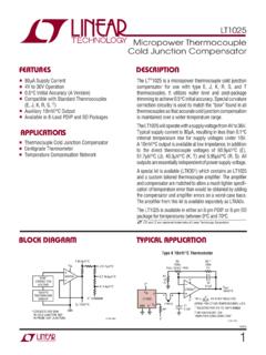
1 LTC2854/LTC28551285455fcFor more information 20 Mbps RS485/RS422 Transceivers with Integrated Switchable TerminationThe LT C 2854 and LTC2855 are low power, 20 Mbps RS485/RS422 transceivers operating on supplies. The receiver includes a logic-selectable 120 termination, one-eighth unit load supporting up to 256 nodes per bus (C-, I-Grade), and a failsafe feature that guarantees a high output state under conditions of floating or shorted driver maintains a high output impedance over the entire common mode range when disabled or when the supply is removed.
2 Excessive power dissipation caused by bus contention or a fault is prevented by current limiting all outputs and by a thermal ESD protection allows the LTC2854 to withstand 25kV (human body model) and the LTC2855 to withstand 15kV on the transceiver interface pins without latchup or damage. nLow Power RS485/RS422 Transceiver nLevel Translator nBackplane Transceiver nIntegrated, Logic-Selectable 120 Termination Resistor Supply Voltage n20 Mbps Maximum Data Rate nNo Damage or Latchup Up to 25kV HBM nHigh Input Impedance Supports 256 Nodes (C-, I-Grade) nOperation Up to 125 C (H-Grade) nGuaranteed Failsafe Receiver Operation Over the Entire Common Mode Range nCurrent Limited Drivers and Thermal Shutdown nDelayed Micropower Shutdown.
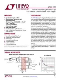
3 5 A Maximum (C-, I-Grade) nPower Up/Down Glitch-Free Driver Outputs nLow Operating Current: 370 A Typical in Receive Mode nCompatible with TIA/EIA-485-A Specifications nAvailable in 10-Pin 3mm 3mm DFN, 12-Pin 4mm 3mm DFN and 16-Pin SSOP PackagesLTC2854 at 20 Mbps into 54 PART NUMBERDUPLEXPACKAGELTC2854 HALFDFN-10 LTC2855 FULLSSOP-16, DFN-12 RETERODEDIRD285455 TA01 LTC2854120 REROTEDEDIRDLTC2854120 REROTE DEDIRDLTC2854120 20ns/DIV2V/DIV285455 TA01bA-BBADIL, LT, LT C, LT M, Linear Technology and the Linear logo are registered trademarks of Linear Technology Corporation.
4 All other trademarks are the property of their respective APPLICATION FEATURESDESCRIPTIONAPPLICATIONSPRODUCT SELECTION GUIDELTC2854/LTC28552285455fcFor more information MAXIMUM RATINGSS upply Voltage (VCC) .. to 7 VLogic Input Voltages (RE, DE, DI, TE) .. to 7 VInterface I /O: A, B, Y , Z ..(VCC 15V) to +15V (A-B) or (B-A) with Terminator Enabled ..6 VReceiver Output Voltage (RO) .. to (VCC + )(Note 1)Operating Temper atur e (Note 4) LTC2854C, LTC2855C ..0 C to 70 C LTC2854I, LTC2855I .. 40 C to 85 C LTC2854H, LTC2855H.
5 40 C to 125 CStorage Temper atur e Range .. 65 C to 150 CLead Temper atur e (Soldering, 10 sec) GN Package ..300 CTOP VIEWDD PACKAGE10-LEAD (3mm 3mm) PLASTIC DFN10967845321 VCCBANCGNDROREDEDITE11 EXPOSED PAD (PIN 11) PCB GND CONNECTIONTJMAX = 150 C, JA = 43 C/W JC = C/W121110987123456 VCCABZYNCROREDEDITEGNDTOP VIEWDE PACKAGE12-LEAD (4mm 3mm) PLASTIC DFN13 EXPOSED PAD (PIN 13) PCB GND CONNECTIONTJMAX = 150 C, JA = 44 C/W JC = C/WROREDEDITEGNDNCNCVCCBZNCNCNCAYGN PACKAGE16-LEAD (NARROW ) PLASTIC SSOP12345678 TOP VIEW161514131211109 TJMAX = 150 C, JA = 110 C/W JC = 40 C/WORDER INFORMATIONLEAD FREE FINISHTAPE AND REELPART MARKING*PACKAGE DESCRIPTIONTEMPERATURE RANGELTC2854 CDD#PBFLTC2854 CDD#TRPBFLCQG10-Lead (3mm 3mm) Plastic DFN0 C to 70 CLTC2854 IDD#PBFLTC2854 IDD#TRPBFLCQG10-Lead (3mm 3mm) Plastic DFN 40 C to 85 CLTC2854 HDD#PBFLTC2854 HDD#TRPBFLCQG10-Lead (3mm 3mm) Plastic DFN 40 C to 125 CLTC2855 CDE#PBFLTC2855 CDE#TRPBF285512-Lead (4mm 3mm)
6 Plastic DFN0 C to 70 CLTC2855 IDE#PBFLTC2855 IDE#TRPBF285512-Lead (4mm 3mm) Plastic DFN 40 C to 85 CLTC2855 HDE#PBFLTC2855 HDE#TRPBF285512-Lead (4mm 3mm) Plastic DFN 40 C to 125 CLTC2855 CGN#PBFLTC2855 CGN#TRPBF285516-Lead (Narrow ) Plastic SSOP0 C to 70 CLTC2855 IGN#PBFLTC2855 IGN#TRPBF2855I16-Lead (Narrow ) Plastic SSOP 40 C to 85 CLTC2855 HGN#PBFLTC2855 HGN#TRPBF2855H16-Lead (Narrow ) Plastic SSOP 40 C to 125 CLEAD BASED FINISHTAPE AND REELPART MARKING*PACKAGE DESCRIPTIONTEMPERATURE RANGELTC2854 CDDLTC2854 CDD#TRLCQG10-Lead (3mm 3mm) Plastic DFN0 C to 70 CLTC2854 IDDLTC2854 IDD#TRLCQG10-Lead (3mm 3mm) Plastic DFN 40 C to 85 CLTC2854 HDDLTC2854 HDD#TRLCQG10-Lead (3mm 3mm) Plastic DFN 40 C to 125 CLTC2855 CDELTC2855 CDE#TR285512-Lead (4mm 3mm) Plastic DFN0 C to 70 CLTC2855 IDELTC2855 IDE#TR285512-Lead (4mm 3mm) Plastic DFN 40 C to 85 CLTC2855 HDELTC2855 HDE#TR285512-Lead (4mm 3mm)
7 Plastic DFN 40 C to 125 CLTC2855 CGNLTC2855 CGN#TR285516-Lead (Narrow ) Plastic SSOP0 C to 70 CLTC2855 IGNLTC2855 IGN#TR2855I16-Lead (Narrow ) Plastic SSOP 40 C to 85 CLTC2855 HGNLTC2855 HGN#TR2855H16-Lead (Narrow ) Plastic SSOP 40 C to 125 CConsult LT C Marketing for parts specified with wider operating temperature ranges. *The temperature grade is identified by a label on the shipping more information on lead free part marking, go to: For more information on tape and reel specifications, go to: CONFIGURATIONLTC2854/LTC28553285455fcFor more information The l denotes the specifications which apply over the full operating temperature range, otherwise specifications are at TA = 25 C, VCC = unless otherwise noted (Note 2).
8 ELECTRICAL CHARACTERISTICSSYMBOLPARAMETERCONDITIONS MINTYPMAXUNITSD river|VOD|Differential Driver Output VoltageR = , VCC = 3V (Figure 1) R = 27 , VCC = 3V (Figure 1) R = 50 , VCC = (Figure 1)l l l 2 VCC VCC VCCV V VD|VOD|Change in Magnitude of Driver Differential Output Voltage for Complementary Output StatesR = 27 or R = 50 (Figure 1) Common Mode Output VoltageR = 27 or R = 50 (Figure 1)l3VD|VOC|Change in Magnitude of Driver Common Mode Output Voltage for Complementary Output StatesR = 27 or R = 50 (Figure 1) Three-State (High Impedance) Output Current on Y and ZDE = OV, (Y or Z) = 7V, 12V (LTC2855) H-Gradel l 10 50 A AIOSD Maximum Driver Short-Circuit Current 7V (Y or Z) 12V (Figure 2) l 250180 250 300mA mAReceiverIINR eceiver Input Current (A, B)DE = TE = 0V, VCC = 0V or , VIN = 12V (Figure 3) (C-, I-Grade) DE = TE = 0V, VCC = 0V or , VIN = 7V, (Figure 3) (C-, I-Grade)
9 L l 100125 A ADE = TE = 0V, VCC = 0V or , VIN = 12V (Figure 3) (H-Grade) DE = TE = 0V, VCC = 0V or , VIN = 7V, (Figure 3) (H-Grade)l l 145250 A ARINR eceiver Input ResistanceRE = VCC or 0V, DE = TE = 0V, VIN = 7V, 3V, 3V, 7V, 12V (Figure 3) (C-, I-Grade)l96125k RE = VCC or 0V, DE = TE = 0V, VIN = 7V, 3V, 3V, 7V, 12V (Figure 3) (H-Grade)l48125k VTHR eceiver Differential Input Threshold Voltage 7V B 12Vl Input HysteresisB = 0V 25mVVOHR eceiver Output HIGH VoltageI(RO) = 4mA, A-B = 200mV, VCC = Output LOW VoltageI(RO) = 4mA, A-B = 200mV, VCC = Three-State (High Impedance) Output Current on RORE = VCC, 0V RO VCCl 1 AIOSRR eceiver Short-Circuit Current0V RO VCCl 85mARTERMR eceiver Input Terminating ResistorTE = VCC, VAB = 2V, VB = 7V, 0V, 10V (Figure 8) l108120156 Logic VIHL ogic Input High VoltageVCC = Input Low VoltageVCC = Input Currentl0 10 ASuppliesICCSS upply Current in Shutdown ModeDE = 0V, RE = VCC, TE = 0V (C-, I-Grade) (H-Grade)
10 L l 0 0 5 15 A AICCRS upply Current in Receive ModeDE = 0V, RE = 0V, TE = 0Vl370900 ALTC2854/LTC28554285455fcFor more information 1: Stresses beyond those listed under Absolute Maximum Ratings may cause permanent damage to the device. Exposure to any Absolute Maximum Rating condition for extended periods may affect device reliability and lifetime. High temperatures degrade operating lifetimes. Operating lifetime is derated at temperatures greater than 105 2: All currents into device pins are positive; all currents out of device pins are negative.
