Transcription of LTC3124 - 15V, 5A 2-Phase Synchronous Step-Up …
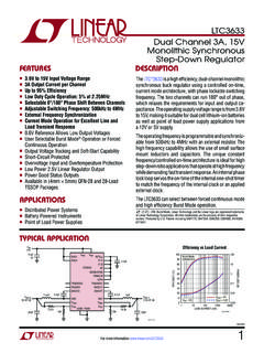
1 LTC312413124fFor more information APPLICATION FEATURESDESCRIPTION15V, 5A 2-Phase Synchronous Step-Up DC/DC Converter with Output DisconnectThe LT C 3124 is a dual-phase, Synchronous Step-Up DC/DC converter with true output disconnect and inrush current limiting capable of providing output voltages up to 15V. Dual-phase operation significantly reduces peak inductor and capacitor ripple currents, minimizing induc-tor and capacitor size. The per phase current limit, along with the ability to program output voltages up to 15V make the LTC3124 well suited for a variety of demanding applications. Once started, operation will continue with inputs down to LTC3124 switching frequency can be programmed from 100kHz to 3 MHz to optimize applications for highest efficiency or smallest solution footprint. The oscillator can be synchronized to an external clock for noise sensitive applications. Selectable Burst Mode operation reduces quiescent current to 25 A, ensuring high efficiency across the entire load range.
2 An internal soft-start limits inrush current during features include a <1 A shutdown current and robust protection under short-circuit, thermal overload, and output overvoltage conditions. The LTC3124 is offered in both 16-lead DFN and thermally-enhanced TSSOP to 12V Synchronous Boost ConverterEfficiency CurveAPPLICATIONSn VIN Range: to , 500mV After Start-Upn Adjustable Output Voltage: to 15Vn Output Current for VIN = 5V and VOUT = 12Vn Dual-Phase Control Reduces Output Voltage Ripplen Output Disconnects from Input When Shut Downn Synchronous Rectification: Up to 95% Efficiencyn Inrush Current Limitn Up to 3 MHz Programmable Switching Frequency Synchronizable to External Clockn Selectable Burst Mode Operation: 25 A IQn Output Overvoltage Protectionn Internal Soft-Startn <1 A IQ in Shutdownn 16-Lead, Thermally- Enhanced 3mm 5mm DFN and TSSOP Packagesn RF, Microwave Power Amplifiersn Piezo Actuatorsn Small DC Motors, Thermal Printersn 12V Analog Rail from Battery, 5V, or Backup CapacitorL, LT , LT C, LT M, Burst Mode, Linear Technology and the Linear logo are registered trademarks and ThinSOT is a trademark of Linear Technology Corporation.
3 All other trademarks are the property of their respective owners. F HVIN5 VSWBCAPPGNDBVOUTBSWALTC3124680pF56pF3124 F10 ONVINSGNDPWM/SYNCSDVCCFBRTVCPGNDAVOUTABU RST CURRENT (mA)EFFICIENCY (%)POWER LOSS (W)3124 ModeOPERATIONB urst ModeOPERATIONEFFICIENCYPOWER LOSSfSW = 1 MHzLTC312423124fFor more information MAXIMUM RATINGSVIN Voltage .. to 6 VVOUTA, VOUTB Voltages .. to 18 VSWA, SWB Voltages (Note 2) .. to 18 VSWA, SWB (Pulsed < 100ns) (Note 2) .. to 19 VVC Voltage .. to VCCRT Voltage .. to VCCCAP Voltage VOUT < .. to (VOUT + ) VOUT (VOUT 6V) to (VOUT + ) VOUT > ..(VOUT 6V) to 12 VAll Other Pins .. to 6 VOperating Junction Temper atur e Range (Notes 3, 4) LTC3124E/ LTC3124I .. 40 C to 125 C LTC3124H .. 40 C to 150 CStorage Temper atur e Range .. 65 C to 150 CLead Temper atur e (Soldering, 10 sec) FE Package Only ..300 C(Note 1)16151413121110917 PGND12345678 CAPVOUTBNCVOUTASGNDSDFBVCSWBPGNDBSWAPGND AVINPWM/SYNCVCCRTTOP VIEWDHC PACKAGE16-LEAD (5mm 3mm) PLASTIC DFN TJMAX = 125 C, JA = 43 C/W (NOTE 5), JC = 5 C/WEXPOSED PAD (PIN 17) IS PGND AND MUST BE SOLDERED TO PCB FOR RATED THERMAL PERFORMANCEFE PACKAGE16-LEAD PLASTIC TSSOP12345678 TOP VIEW161514131211109 SWBPGNDBSWAPGNDAVINPWM/SYNCVCCRTCAPVOUTB NCVOUTASGNDSDFBVC17 PGND TJMAX = 150 C, JA = 40 C/W (NOTE 5), JC = 10 C/WEXPOSED PAD (PIN 17) IS PGND AND MUST BE SOLDERED TO PCB FOR RATED THERMAL PERFORMANCEPIN CONFIGURATIONORDER INFORMATIONLEAD FREE FINISHTAPE AND REELPART MARKING*PACKAGE DESCRIPTIONTEMPERATURE RANGELTC3124 EDHC#PBFLTC3124 EDHC#TRPBF312416-Lead (5mm 3mm) Plastic DFN 40 C to 125 CLTC3124 IDHC#PBFLTC3124 IDHC#TRPBF312416-Lead (5mm 3mm)
4 Plastic DFN 40 C to 125 CLTC3124 EFE#PBFLTC3124 EFE#TRPBF3124FE16-Lead Plastic TSSOP 40 C to 125 CLTC3124 IFE#PBFLTC3124 IFE#TRPBF3124FE16-Lead Plastic TSSOP 40 C to 125 CLTC3124 HFE#PBFLTC3124 HFE#TRPBF3124FE16-Lead Plastic TSSOP 40 C to 150 CConsult LT C Marketing for parts specified with wider operating temperature ranges. *The temperature grade is identified by a label on the shipping LT C Marketing for information on non-standard lead based finish more information on lead free part marking, go to: For more information on tape and reel specifications, go to: more information CHARACTERISTICSNote 1: Stresses beyond those listed under Absolute Maximum Ratings may cause permanent damage to the device. Exposure to any Absolute Maximum Rating condition for extended periods may affect device reliability and 2: Voltage transients on the SW pin beyond the DC limit specified in the Absolute Maximum Ratings are non-disruptive to normal operations when using good layout practices, as shown on the demo board or described in the data sheet or application 3: The LTC3124 is tested under pulsed load conditions such that TA TJ.
5 The LTC3124E is guaranteed to meet performance specifications from 0 C to 85 C junction temperature. Specifications over the 40 C to 125 C operating junction temperature range are assured by design, characterization and correlation with statistical process controls. The LTC3124I is guaranteed to meet specifications over the 40 C to 125 C operating junction temperature range. The LTC3124H is guaranteed to meet specifications over the full 40 C to 150 C operating junction range. High junction temperatures degrade operating lifetimes; operating lifetime is derated for junction temperatures greater than 125 that the maximum ambient temperature consistent with these specifications is determined by specific operating conditions in conjunction with board layout, the rated package thermal impedance and other environmental factors. The junction temperature (TJ in C) is calculated from the ambient temperature (TA in C) and power dissipation (PD in Watts) according to the formula: TJ = TA + (PD JA) where JA is the thermal impedance of the 4: The LTC3124 includes overtemperature protection that is intended to protect the device during momentary overload conditions.
6 Junction temperature will exceed 150 C when overtemperature shutdown is active. Continuous operation above the specified maximum operating junction temperature may result in device degradation or 5: Failure to solder the exposed backside of the package to the PC board ground plane will result in a thermal impedance much higher than the rated package specifications. The l denotes the specifications which apply over the specified operating junction temperature range, otherwise specifications are at TA = 25 C (Note 3). VIN = , VOUTA = VOUTB = 12V, RT = 28k unless otherwise Start-Up VoltageVOUT = Voltage RangeVOUT Voltage Adjust Input CurrentFB = Current, ShutdownSD = 0V, VOUT = 0V, Not Including Switch AQuiescent Current, ActiveFB = , Measured on VIN, Non-Switching600840 AQuiescent Current, BurstMeasured on VIN, FB = Measured on VOUT, FB = 1040 20 A AN-Channel MOSFET Switch Leakage CurrentSW = 15V, VOUT = 15V, Per AP-Channel MOSFET Switch Leakage CurrentSW = 0V, VOUT = 15V, SD = 0V, Per AN-Channel MOSFET Switch On-ResistancePer P-Channel MOSFET Switch On-ResistancePer N-Channel MOSFET Peak Current LimitPer Duty CycleFB = Duty CycleFB = FrequencyPer Frequency Input High VCCVPWM/SYNC Input Low VCCVPWM/SYNC Input CurrentVPWM/SYNC = ACAP Clamp VoltageVOUT > , Referenced to VOUT Regulation VoltageVIN < , VOUT > Amplifier Transconductancel60100130 SError Amplifier Sink CurrentFB =.
7 VC = AError Amplifier Source CurrentFB = 800mV, VC = 25 ASoft-Start Time10msSD Input High Input Low Voltage Input CurrentSD = ALTC312443124fFor more information PERFORMANCE CHARACTERISTICSPWM Mode OperationLoad Transient ResponseInrush Current ControlFeedback vs TemperatureRDS(ON) vs Temperature, Both NMOS and PMOSS witching Frequency vs TemperatureEfficiency vs Load Current, VOUT = 5 VEfficiency vs Load Current, VOUT = vs Load Current, VOUT = 12V1001090705030806040200 LOAD CURRENT (mA)EFFICIENCY (%)3124 = = = ModeOPERATIONfSW = 1 MHz1001090705030806040200 LOAD CURRENT (mA)EFFICIENCY (%)3124 = = = ModeOPERATIONfSW = 1 MHz1001090705030806040200 LOAD CURRENT (mA)EFFICIENCY (%)3124 = = = ModeOPERATIONfSW = 1 MHzTEMPERATURE ( C) 50 CHANGE IN RDS(ON) FROM 25 C (%)806040200 20 4070110 103124 G0830150 VOUT20mV/DIVAC-COUPLEDPHASE AINDUCTORCURRENT500mA/DIVPHASE BINDUCTORCURRENT500mA/DIV2 s/DIVILOAD = 500mA3124 G04 VOUT500mV/DIVAC-COUPLEDOUTPUTCURRENT500m A/DIV500 s/DIVRC = 169kCC = 330pFNO CF3124 G05150mA150mA1500mASD5V/DIVVOUT5V/DIVIND UCTOR ACURRENT1A/DIVINDUCTOR BCURRENT1A/DIV2ms/DIVILOAD = 100mA3124 G06 TEMPERATURE ( C) 40 CHANGE IN VFB FROM 25 C (%) G07 ( C) 50 20 IN FREQUENCY FROM 25 C (%) G09 as front page application at TA = 25 C, unless otherwise more information PERFORMANCE CHARACTERISTICSB urst Mode Output Current vs VINB urst Mode No-Load Input Current vs VINB urst Mode Quiescent Current Change vs TemperatureSD Pin ThresholdPWM Mode Maximum Output Current vs VINPeak Current Limit Changevs TemperaturePWM Operation No-Load Input Current vs VINVIN (V)1 OUTPUT CURRENT (A) = 5 VVOUT = = 12 VVOUT = 15 VTEMPERATURE ( C) 50 PEAK CURRENT LIMIT CHANGE FROM 25 C (%)
8 210 1 2 3 470110 103124 G1130150 VIN (V)1 INPUT CURRENT (mA)12016020053124 = 15 VVOUT = 12 VVOUT = = 5 VVOUT = , FALLING (V)1 OUTPUT CURRENT (mA)30040053124 = = 5 VVOUT = = 12 VVOUT = 15 VVIN, FALLING (V) CURRENT ( A) G1410 VOUT = 15 VVOUT = 12 VVOUT = = 5 VVOUT = G16 VOUT5V/DIVVSD500mV/DIV900mV400mVRT vs FrequencyConfigured as front page application at TA = 25 C, unless otherwise (kHz)10010RT RESISTANCE (k )10100100030003124 G17 TEMPERATURE ( C) 50 CHANGE IN CURRENT FROM 25 C (%)75604530150 1570110 103124 G1530150 LTC312463124fFor more information PERFORMANCE CHARACTERISTICSB urst Mode OperationBurst Mode Operation to PWM ModePWM Mode to Burst Mode OperationBurst Mode TransientSynchronized OperationEfficiency vs FrequencyFrequency AccuracyCAP Pin Voltage vs VOUTVCC vs VINVIN, FALLING (V) IN FREQUENCY (%)013124 G19 1 = 15 VVOUT = = (V)0 VCAP, REFERRED TO VOUT (V)0 3 4 5 2 1 6 7106423124 G2181412 VIN (V)0 VCC (V) G22365 VIN FALLINGVIN RISINGVOUT100mV/DIVAC-COUPLEDVSWA10V/DIV PHASE AINDUCTORCURRENT500mA/DIV5 s/DIVOUTPUT CURRENT = 50mA3124 G23 VOUT50mV/DIVAC-COUPLEDVPWM/SYNC2V/DIV50 s/DIVOUTPUT CURRENT = 100mATYPE III COMPENSATION SEE FIGURE 10 FORCOMPONENT VALUES3124 G25 VOUT100mV/DIVAC-COUPLEDOUTPUTCURRENT100m A/DIV200 s/DIV3124 G26100mA10mA10mAVSWB10V/DIVVSWA10V/DIVVP WM/SYNC5V/DIV1 s/DIVOUTPUT CURRENT = 1A3124 G27 SYNCHRONIZATION SIGNAL SET TO TO CURRENT (mA)1040 EFFICIENCY (%)5060708010010003124 G20302010090100100kHz EFFICIENCY1 MHz EFFICIENCY3 MHz EFFICIENCYVOUT50mV/DIVAC-COUPLEDVPWM/SYN C2V/DIV50 s/DIVOUTPUT CURRENT = 100mATYPE III COMPENSATION SEE FIGURE 10 FORCOMPONENT VALUES3124 G24 Configured as front page application at TA = 25 C, unless otherwise more information PERFORMANCE CHARACTERISTICSO utput Voltage Ripple at Load with Two 10 F Ceramic CapacitorsSWA and SWB at 1 MHz/PhaseSW Pins while Synchronizing to ResponsePIN FUNCTIONSSWB, SWA (Pin 1, Pin 3).
9 Phase B and Phase A Switch Pins. Connect inductors from these pins to the input sup-ply. Keep PCB trace lengths as short and wide as possible to reduce EMI and voltage overshoot. When VOUT VIN + 2V, internal anti-ringing resistors are connected between VIN and both SWA and SWB after their respective induc-tor currents have dropped to near zero, to minimize EMI. These anti-ringing resistors are also activated in shutdown and during the sleep periods of Burst Mode , PGNDA, PGND (Pin 2, Pin 4, Exposed Pad Pin 17): Power Ground. When laying out your PCB, provide a short, direct path between PGND and the output capaci-tors and tie directly to the ground plane. The exposed pad is ground and must be soldered to the PCB ground plane for rated thermal and electrical (Pin 5): Input Supply Pin. The device is powered from VIN if VIN is initially greater than approximately , with VIN continuing to supply the device down to approximately 3V; otherwise the greater of VIN and VOUT supplies the Configured as front page application at TA = 25 C, unless otherwise BCURRENT2A/DIVINDUCTOR ACURRENT2A/DIV100 s/DIVILOAD = 500mA3124 G28 SHORT-CIRCUITAPPLIEDSHORT-CIRCUITREMOVED VSWA5V/DIVVSWB5V/DIV500ns/DIVILOAD = 1500mA3124 G29 INDUCTOR BCURRENT500mA/DIVINDUCTOR ACURRENT500mA/DIVVOUT20mV/DIVAC-COUPLED5 00ns/DIV3124 G31 VSWA5V/DIVVSWB5V/DIV500ns/DIVILOAD = 1500mA3124 G30 LTC312483124fFor more information FUNCTIONS device.
10 Place a low ESR ceramic bypass capacitor of at least 10 F from VIN to PGND. X5R and X7R dielectrics are preferred for their superior voltage and temperature (Pin 6): Burst Mode Operation Select and Oscillator Synchronization. Do not leave this pin floating. PWM/SYNC = High. Disable Burst Mode operation and maintain low noise, constant frequency operation. PWM/SYNC = Low. The converter operates in Burst Mode, independent of load current. PWM/SYNC = External CLK. The internal oscillator is synchronized to the external CLK signal. Burst Mode operation is disabled. A clock pulse width of 100ns minimum is required to synchronize the oscillator. An external resistor MUST BE connected between RT and SGND to program the oscillator slightly below the desired synchronization non-synchronized applications, repeated clocking of the PWM/SYNC pin to affect an operating mode change is supported with these restrictions: Boost Mode (VOUT > VIN): IOUT < 3mA: fPWM/SYNC 10Hz, IOUT 3mA: fPWM/SYNC 5kHz.