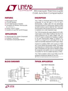
Transcription of LTC3633 - Dual Channel 3A, 15V Monolithic …
1 LTC363313633fdFor more information APPLICATION FEATURESDESCRIPTIONDual Channel 3A, 15V Monolithic synchronous step - down RegulatorThe LT C 3633 is a high efficiency, dual - Channel Monolithic synchronous buck regulator using a controlled on-time, current mode architecture, with phase lockable switching frequency. The two channels can run 180 out of phase, which relaxes the requirements for input and output ca-pacitance. The operating supply voltage range is from to 15V, making it suitable for dual cell lithium-ion batteries as well as point of load power supply applications from a 12V or 5V operating frequency is programmable and synchroniz-able from 500kHz to 4 MHz with an external resistor.
2 The high frequency capability allows the use of small surface mount inductors and capacitors. The unique constant frequency/controlled on-time architecture is ideal for high step - down ratio applications that operate at high frequency while demanding fast transient response. An internal phase lock loop servos the on-time of the internal one-shot timer to match the frequency of the internal clock or an applied external LTC3633 can select between forced continuous mode and high efficiency Burst Mode , LT, LTC, LTM, Burst Mode, Linear Technology and the Linear logo are registered trademarks of Linear Technology Corporation.
3 All other trademarks are the property of their respective owners. Protected by Patents including 5481178, 5847554, 6580258, 6304066, 6476589, to 15V Input Voltage Rangen 3A Output Current per Channeln Up to 95% Efficiencyn Low Duty Cycle Operation: 5% at Selectable 0 /180 Phase Shift Between Channelsn Adjustable Switching Frequency: 500kHz to 4 MHzn External Frequency Synchronizationn Current Mode Operation for Excellent Line and Load Transient Responsen Reference Allows Low Output Voltagesn User Selectable Burst Mode Operation or Forced Continuous Operationn Output Voltage Tracking and Soft-Start Capabilityn Short-Circuit Protectedn Overvoltage Input and Overtemperature Protectionn Low Power Linear Regulator Outputn Power Good Status Outputsn Available in (4mm 5mm)
4 QFN-28 and 28-Lead TSSOP Packagesn Distributed Power Systemsn Battery Powered Instrumentsn Point of Load Power SuppliesEfficiency vs Load Current10 EFFICIENCY (%)POWER LOSS (W)1030405070100100003633 = 5 VVOUT = CURRENT (mA)Burst ModeOPERATIONVIN = FVOUT2 5V AT F1 AT 3 AVIN 12V47 Fx2 F3633 TA01aLTC363323633fdFor more information MAXIMUM RATINGSVIN1, VIN2 .. to 16 VVIN1, VIN2 Tr ansi en t ..18 VPGOOD1, PGOOD2, VON1, VON2 .. to 16 VBOOST1, BOOST2 .. to , BOOST2-SW2 .. to , INTVCC, TRACKSS1, TRACKSS2 .. to , ITH2, RT, MODE/SYNC .. to INTVCC + , VFB2, PHMODE.
5 To INTVCC + , RUN2 .. to VIN + Junction Temperature Range (Notes 2, 3) .. 40 C to 125 CStorage Temperature Range .. 65 C to 125 C(Note 1)910 TOP VIEWUFD PACKAGE28-LEAD (4mm 5mm) PLASTIC QFN11121328 27 26 25 241423654321 PGOOD1 PHMODERUN1 MODE/SYNCRTRUN2 SGNDPGOOD2 VIN1 VIN1 BOOST1 INTVCCV2P5 BOOST2 VIN2 VIN2 VFB1 TRACKSS1 ITH1 VON1SW1SW1 VFB2 TRACKSS2 ITH2 VON2SW2SW271718192021221681529 PGND TJMAX = 125 C, JA = 43 C/W EXPOSED PAD (PIN 29) IS PGND, MUST BE SOLDERED TO PCB1234567891011121314 TOP VIEWFE PACKAGE28-LEAD PLASTIC TSSOP2827262524232221201918171615 ITH1 TRACKSS1 VFB1 PGOOD1 PHMODERUN1 MODE/SYNCRTRUN2 SGNDPGOOD2 VFB2 TRACKSS2 ITH2 VON1SW1SW1 VIN1 VIN1 BOOST1 INTVCCV2P5 BOOST2 VIN2 VIN2SW2SW2 VON229 PGND TJMAX = 125 C, JA = 25 C/W EXPOSED PAD (PIN 29) IS PGND, MUST BE SOLDERED TO PCBPIN CONFIGURATIONORDER INFORMATIONLEAD FREE FINISHTAPE AND REELPART MARKING*PACKAGE DESCRIPTIONTEMPERATURE RANGELTC3633 EUFD#PBFLTC3633 EUFD#TRPBF363328-Lead (4mm 5mm)
6 Plastic QFN 40 C to 125 CLTC3633 IUFD#PBFLTC3633 IUFD#TRPBF363328-Lead (4mm 5mm) Plastic QFN 40 C to 125 CLTC3633 EFE#PBFLTC3633 EFE#TRPBFLTC3633FE28-Lead Plastic TSSOP 40 C to 125 CLTC3633 IFE#PBFLTC3633 IFE#TRPBFLTC3633FE28-Lead Plastic TSSOP 40 C to 125 CConsult LTC Marketing for parts specified with wider operating temperature ranges. *The temperature grade is identified by a label on the shipping container. Consult LTC Marketing for information on non-standard lead based finish more information on lead free part marking, go to: For more information on tape and reel specifications, go to: more information The l denotes the specifications which apply over the full operating junction temperature range, otherwise specifications are at TJ = 25 C (Note 2).
7 VIN1 = VIN2 = 12V, unless otherwise CHARACTERISTICSSYMBOLPARAMETERCONDITIONS MINTYPMAXUNITSVINS upply DC Supply Current (VIN1 + VIN2) Both Channels Active (Note 4) Sleep Current Shutdown MODE = 0V MODE = INTVCC, VFB1, VFB2 > RUN1 = RUN2 = 0V 500 13 mA A AVFBF eedback Reference VLINE_REGR eference Voltage Line RegulationVIN = to VLOAD_REGO utput Voltage Load RegulationITH = to Pin Input Current 30nAgm(EA)Error Amplifier Transconductance ITH = On TimeVON = 1V, VIN = 4V20nstOFFM inimum Off TimeVIN = 6V4060nsfOSCO scillator FrequencyVRT = INTVCC RT = 160k RT = 2 MHz MHzILIMP ositive Valley Switch Current Valley Switch Current Limit 2 ARDS(ON)Top Switch On-Resistance Bottom Switch On-Resistance130 65m m ISW(LKG)
8 Switch Leakage CurrentVIN = 15V, VRUN = 1 AVVIN-OVVIN Overvoltage Lockout ThresholdVIN Rising VIN 17V VINTVCC < VIN < 15V, 0mA Load Regulation0mA to 50mA Load, VIN = 4V to Threshold Rising RUN Threshold Fallingl VRUN Leakage CurrentVIN = 15V0 3 AV2P5 VoltageILOAD = 0mA to Good-to-Bad ThresholdVFB Rising VFB Falling 8 810 10% %PGOOD Bad-to-Good ThresholdVFB Rising VFB Falling 3 3 5 5% %RPGOODPGOOD Pull- down Resistance10mA Load15 tPGOODP ower Good Filter Time2040 stSSInternal Soft-Start Time10% to 90% Rise Time400700 sVFB During TrackingTRACKSS = Pull-Up AVPHMODEPHMODE Threshold VoltagePHMODE VIH PHMODE VIL1 VVMODE/SYNCMODE/SYNC Threshold VoltageMODE VIH MODE VIL1 VSYNC Threshold VoltageSYNC Input CurrentMODE = 0V MODE =
9 A ALTC363343633fdFor more information CHARACTERISTICSNote 1: Stresses beyond those listed under Absolute Maximum Ratings may cause permanent damage to the device. Exposure to any Absolute Maximum Rating condition for extended periods may affect device reliability and 2: The LTC3633 is tested under pulsed load conditions such that TJ TA. The LTC3633E is guaranteed to meet performance specifications from 0 C to 85 C junction temperature. Specifications over the 40 C to 125 C operating junction temperature range are assured by design, characterization and correlation with statistical process controls.
10 The LTC3633I is guaranteed over the full 40 C to 125 C operating junction temperature range. Note that the maximum ambient temperature consistent with these specifications is determined by specific operating conditions in conjunction with board layout, the rated package thermal impedance and other environmental factors. The junction temperature (TJ, in C) is calculated from the ambient temperature (TA, in C) and power dissipation (PD, in watts) according to the formula: TJ = TA + (PD JA), where JA (in C/W) is the package thermal 3: This IC includes overtemperature protection that is intended to protect the device during momentary overload conditions.
