Transcription of LTC3780 (Rev G) - Analog Devices
1 LTC37801 Rev GFor more information FeedbackTYPICAL APPLICATIONFEATURESAPPLICATIONSDESCRIPTI ONHigh efficiency , Synchronous, 4-Switch buck -Boost ControllerThe LT C 3780 is a high performance buck -boost switch-ing regulator controller that operates from input voltages above, below or equal to the output voltage. The constant frequency current mode architecture allows a phase-lockable frequency of up to 400kHz. With a wide 4V to 30V (36V maximum) input and output range and seamless transfers between operating modes, the LTC3780 is ideal for automotive, telecom and battery-powered operating mode of the controller is determined through the FCB pin.
2 For boost operation, the FCB mode pin can select among Burst Mode operation, discontinuous mode and forced continuous mode. During buck operation, the FCB mode pin can select among skip-cycle mode, discon-tinuous mode and forced continuous mode. Burst Mode operation and skip-cycle mode provide high efficiency operation at light loads while forced continuous mode and discontinuous mode operate at a constant frequency. Fault protection is provided by an output overvoltage comparator and internal foldback current limiting. A power good output pin indicates when the output is within of its designed set efficiency buck -Boost Convertern single Inductor Architecture Allows VIN Above, Below or Equal to VOUTn Wide VIN Range: 4V to 36V Operationn Synchronous Rectification: Up to 98% Efficiencyn Current Mode Controln 1% Output Voltage Accuracy: < VOUT < 30Vn Phase-Lockable Fixed Frequency.
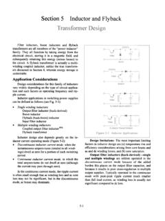
3 200kHz to 400kHzn Power Good Output Voltage Monitorn Internal LDO for MOSFET Supplyn Quad N-Channel MOSFET Synchronous Driven VOUT Disconnected from VIN During Shutdownn Adjustable Soft-Start Current Rampingn Foldback Output Current Limitingn Selectable Low Current Modesn Output Overvoltage Protectionn Available in 24-Lead SSOP and Exposed Pad (5mm 5mm) 32-Lead QFN Packagesn Automotive Systemsn Telecom Systemsn DC Power Distribution Systemsn high Power Battery-Operated Devicesn Industrial Control+ FABDC2200pF1 FCER100 F16 VCER330 F16 H20kPGOODLTC3780 INTVCCSENSE+SENSE TA01105k1%22 F50 VCERVIN5V TO 32 VVOUT12V5A+VIN (V)0 efficiency (%)POWER LOSS (W)909510015253780 TA01b85805102030357570891076543210 efficiency and Power LossVOUT = 12V, ILOAD = 5 AAll registered trademarks and trademarks are the property of their respective owners.
4 Protected by Patents, including 5481178, 6304066, 5929620, 5408150, 6580258, patent pending on current mode architecture and GFor more information MAXIMUM RATINGSI nput Supply Voltage (VIN) .. to 36 VTopside Driver Voltages (BOOST1, BOOST2).. to 42 VSwitch Voltage (SW1, SW2) .. 5V to 36 VINTVCC, EXTVCC, (BOOST SW1),(BOOST2 SW2), PGOOD .. to 7 VRUN, SS .. to 6 VPLLIN Voltage .. to Voltage .. to , STBYMD Voltages .. to INTVCC(Note 1)ITH, VOSENSE Voltages .. to Output Current <10 s (TG1, TG2, BG1, BG2) ..3 AINTVCC Peak Output Current .. 40mA Operating Junction Temperature Range (Notes 2, 7) LTC3780E .. 40 C to 85 C LTC3780I.
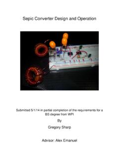
5 40 C to 125 C LTC3780MP .. 55 C to 125 CStorage Temperature Range .. 65 C to 125 CLead Temperature (Soldering, 10 sec) SSOP Only ..300 C123456789101112 TOP VIEWG PACKAGE24-LEAD PLASTIC SSOPTJMAX = 125 C, JA = 130 C/W242322212019181716151413 PGOODSSSENSE+SENSE ITHVOSENSESGNDRUNFCBPLLFLTRPLLINSTBYMDBO OST1TG1SW1 VINEXTVCCINTVCCBG1 PGNDBG2SW2TG2 BOOST232313029282726259101112 TOP VIEW33UH PACKAGE32-LEAD (5mm 5mm) PLASTIC QFNTJMAX = 125 C, JA = 34 C/WEXPOSED PAD (PIN 33) IS SGND, MUST BE SOLDERED TO PCB13141516171819202122232487654321 SENSE+SENSE ITHVOSENSESGNDRUNFCBPLLFTRSW1 VINEXTVCCINTVCCBG1 PGNDBG2SW2 NCSS PGOOD NCNCBOOST1TG1 NCNCPLLINSTBYMDNCNCBOOST2TG2 NCPIN CONFIGURATIONLTC37803 Rev GFor more information CHARACTERISTICS The l denotes the specifications which apply over the full operating junction temperature range, otherwise specifications are at TA = 25 C.
6 (Note 7) VIN = 15V unless otherwise Control LoopVOSENSEF eedback Reference VoltageITH = , 40 C T 85 C (Note 3) 55 C T 125 Cl VIVOSENSEF eedback Pin Input Current(Note 3) 5 50nAVLOADREGO utput Voltage Load Regulation(Note 3) ITH = to ITH = to l l % %VREF(LINEREG)Reference Voltage Line RegulationVIN = 4V to 30V, ITH = (Note 3) (EA)Error Amplifier TransconductanceITH = , Sink/Source = 3 A (Note 3) (GBW)Error Amplifier GBW(Note 8) DC Supply Current Normal Standby Shutdown Supply Current(Note 4) VRUN = 0V, VSTBYMD > 2V VRUN = 0V, VSTBYMD = Open 2400 1500 55 70 A A AVFCBF orced Continuous Continuous Pin CurrentVFCB = AVBINHIBITB urst Inhibit (Constant Frequency) Threshold Measured at FCB ResetVIN Overvoltage LockoutMeasured at VOSENSE Pins Total Source CurrentVSENSE = VSENSE+ = 0V 380 AVSTBYMD(START)Start-Up ThresholdVSTBYMD (KA)
7 Keep-Alive Power-On ThresholdVSTBYMD Rising, VRUN = INFORMATIONLEAD FREE FINISHTAPE AND REELPART MARKINGPACKAGE DESCRIPTIONTEMPERATURE RANGELTC3780EG#PBFLTC3780EG#TRPBFLTC3780 EG24-Lead Plastic SSOP 40 C to 85 CLTC3780IG#PBFLTC3780IG#TRPBFLTC3780IG24 -Lead Plastic SSOP 40 C to 125 CLTC3780 MPG#PBFLTC3780 MPG#TRPBFLTC3780 MPG24-Lead Plastic SSOP 55 C to 125 CLTC3780 EUH#PBFLTC3780 EUH#TRPBF378032-Lead (5mm 5mm) Plastic QFN 40 C to 85 CLTC3780 IUH#PBFLTC3780 IUH#TRPBF3780I32-Lead (5mm 5mm) Plastic QFN 40 C to 125 CLEAD BASED FINISHTAPE AND REELPART MARKINGPACKAGE DESCRIPTIONTEMPERATURE RANGELTC3780 EGLTC3780EG#TRLTC3780EG24-Lead Plastic SSOP 40 C to 85 CLTC3780 IGLTC3780IG#TRLTC3780IG24-Lead Plastic SSOP 40 C to 125 CLTC3780 MPGLTC3780 MPG#TRLTC3780 MPG24-Lead Plastic SSOP 55 C to 125 CLTC3780 EUHLTC3780 EUH#TR378032-Lead (5mm 5mm) Plastic QFN 40 C to 85 CLTC3780 IUHLTC3780 IUH#TR3780I32-Lead (5mm 5mm) Plastic QFN 40 C to 125 CContact the factory for parts specified with wider operating temperature and reel specifications.
8 Some packages are available in 500 unit reels through designated sales channels with #TRMPBF GFor more information CHARACTERISTICS The l denotes the specifications which apply over the full operating junction temperature range, otherwise specifications are at TA = 25 C. (Note 7) VIN = 15V unless otherwise MAX, BoostMaximum Duty Factor% Switch C On99%DF MAX, BuckMaximum Duty Factor% Switch A On (in Dropout)99%VRUN(ON)RUN Pin On ThresholdVRUN Charge CurrentVRUN = AVSENSE(MAX)Maximum Current Sense ThresholdBoost: VOSENSE = VREF 50mV buck .
9 VOSENSE = VREF 50mV l l120 95 160 110 185 150mV mVVSENSE(MIN, buck )Minimum Current Sense ThresholdDiscontinuous Mode 6mVTG1, TG2 trTG Rise TimeCLOAD = 3300pF (Note 5)50nsTG1, TG2 tfTG Fall TimeCLOAD = 3300pF (Note 5)45nsBG1, BG2 trBG Rise TimeCLOAD = 3300pF (Note 5)45nsBG1, BG2 tfBG Fall TimeCLOAD = 3300pF (Note 5)55nsTG1/BG1 t1 DTG1 Off to BG1 On Delay, Switch C On DelayCLOAD = 3300pF Each Driver80nsBG1/TG1 t2 DBG1 Off to TG1 On Delay, Synchronous Switch D On DelayCLOAD = 3300pF Each Driver80nsTG2/BG2 t3 DTG2 Off to BG2 On Delay, Synchronous Switch B On DelayCLOAD = 3300pF Each Driver80nsBG2/TG2 t4 DBG2 Off to TG2 On Delay, Switch A On Delay CLOAD = 3300pF Each Driver80nsMode Transition 1BG1 Off to BG2 On Delay, Switch A On Delay CLOAD = 3300pF Each Driver250nsMode Transition 2BG2 Off to BG1 On Delay, Synchronous Switch D On DelayCLOAD = 3300pF Each Driver250nstON(MIN,BOOST)Minimum On-Time for Main Switch in Boost OperationSwitch C (Note 6)200nstON(MIN, buck )
10 Minimum On-Time for Synchronous Switch in buck OperationSwitch B (Note 6)180nsInternal VCC RegulatorVINTVCCI nternal VCC Voltage7V < VIN < 30V, VEXTVCC = VLDO(LOADREG)Internal VCC Load RegulationICC = 0mA to 20mA, VEXTVCC = Switchover VoltageICC = 20mA, VEXTVCC VEXTVCC(HYS)EXTVCC Switchover Hysteresis300mV VEXTVCCEXTVCC Switch Drop VoltageICC = 20mA, VEXTVCC = 6V150300mVOscillator and Phase-Locked LoopfNOMN ominal FrequencyVPLLFLTR = FrequencyVPLLFLTR = 0V170200220kHzfHIGHH ighest FrequencyVPLLFLTR = Input Resistance50k IPLLLPFP hase Detector Output CurrentfPLLIN < fOSC fPLLIN > fOSC (Note 9) 15 15 A ALTC37805 Rev GFor more information 1: Stresses beyond those listed under Absolute Maximum Ratings may cause permanent damage to the device.