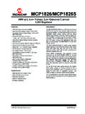
Transcription of MC78L00A - 100 mA Positive Voltage Regulators
1 Semiconductor Components Industries, LLC, 1999 October, 2016 Rev. 181 Publication Order Number: MC78L00A /DMC78L00A series ,NCV78L00A100 mA Positive VoltageRegulatorsThe MC78L00A series of Positive Voltage Regulators areinexpensive, easy to use devices suitable for a multitude ofapplications that require a regulated supply of up to 100 mA. Liketheir higher powered MC7800 and MC78M00 series cousins, theseregulators feature internal current limiting and thermal shutdownmaking them remarkably rugged. No external components arerequired with the MC78L00 devices in many devices offer a substantial performance advantage over thetraditional zener diode resistor combination, as output impedanceand quiescent current are substantially Wide Range of Available, Fixed Output Voltages Low Cost Internal Short Circuit Current Limiting Internal Thermal Overload Protection No External Components Required Complementary Negative Regulators Offered (MC79L00A series ) NCV Prefix for Automotive and Other Applications RequiringUnique Site and Control Change Requirements.
2 AEC Q100 Qualified and PPAP Capable These are Pb Free DevicesFigure 1. Representative Schematic 92P SUFFIXCASE 029 See detailed ordering and shipping information in the packagedimensions section on page 9 of this data INFORMATIONPin: 1. Output2. Ground3. InputPIN CONNECTIONS18765234(Top View)VOUTGNDGNDVINGNDNCGNDNCSOIC 8*D SUFFIXCASE 751*SOIC 8 is an internally modified SO 8 package. Pins2, 3, 6, and 7 are electrically common to the die attachflag. This internal lead frame modification decreasespackage thermal resistance and increases powerdissipation capability when appropriately mounted ona printed circuit board.
3 SOIC 8 conforms to all ex-ternal dimensions of the standard SO 8 general marking information in the device markingsection on page 12 of this data MARKING INFORMATION12312 BENT LEADTAPE & REELAMMO PACKSTRAIGHT LEADBULK PACK3 SOT 89 CASE 528AG123 VOUTGND VINTAB(Top View) series , 2. Standard ApplicationA common ground is required between the input and the output voltages. The input Voltage must remain typically V above the outputvoltage even during the low point on the input ripple Voltage .* Cin is required if regulator is located an appreciable distance from power supply filter.** CO is not needed for stability; however, it does improve transient * mFCO** mFOutputABSOLUTE MAXIMUM RATINGSR atingSymbolValueUnitInput Voltage ( V V)Input Voltage (12 V 18 V)Input Voltage (24 V)VI303540 VdcStorage Temperature RangeTstg 65 to +150 CMaximum Junction TemperatureTJ150 CMoisture Sensitivity LevelMSL1 ESD Capability, Human Body Model (Note 1)ESDHBM2000 VESD Capability, Machine Model (Note 1)ESDMM200 VESD Capability, Charged Device Model (Note 1)ESDCDM2000 VStresses exceeding those listed in the Maximum Ratings table may damage the device.
4 If any of these limits are exceeded, device functionalityshould not be assumed, damage may occur and reliability may be This device series incorporates ESD protection and is tested by the following methods:ESD Human Body Model tested per AEC Q100 002 (EIA/JESD22 A114)ESD Machine Model tested per AEC Q100 003 (EIA/JESD22 A115)ESD Charged Device Model tested per EIA/JES D22/C101, Field Induced Charge CHARACTERISTICSR atingSymbolValueUnitPackage DissipationPDInternally LimitedWThermal Characteristics, TO 92 Thermal Resistance, Junction to AmbientRqJA200 C/WThermal Characteristics, SOIC8 Thermal Resistance, Junction to AmbientRqJARefer to Figure 8 C/WThermal Characteristics, SOT 89 Thermal Resistance, Junction to AmbientRqJA55 C/W2.
5 Thermal Resistance, Junction to Ambient depends on Copper area. See details in Figure Resistance, Junction to Case is not defined. SOIC 8 lead and TO-92 packages that do not have a heat sink like other packagesmay have. This is the reason that a Theta JC is never specified. A little heat transfer will occur through the package but since it is plastic, it isminimal. The majority of the heat that is transferred is through the leads where they connect to the circuit series , CHARACTERISTICS (VI = 10 V, IO = 40 mA, CI = mF, CO = mF, 4 0 C < TJ < +125 C (for MC78 LXXAB,NCV78L05A), 0 C < TJ < +125 C (for MC78 LXXAC), unless otherwise noted.)
6 MC78L05AC, AB, NCV78L05 ACharacteristicsSymbolMinTypMaxUnitOutpu t Voltage (TJ = +25 C) Regulation(TJ = +25 C, IO = 40 mA) Vdc VI 20 Vdc VI 20 VdcRegline 5545150100mVLoad Regulation(TJ = +25 C, mA IO 100 mA)(TJ = +25 C, mA IO 40 mA)Regload Voltage ( Vdc VI 20 Vdc, mA IO 40 mA)(VI = 10 V, mA IO 70 mA) Bias Current(TJ = +25 C)(TJ = +125 C)IIB Bias Current Change( Vdc VI 20 Vdc)( mA IO 40 mA)DIIB Noise Voltage (TA = +25 C, 10 Hz f 100 kHz)Vn 40 mVRipple Rejection (IO = 40 mA,f = 120 Hz, Vdc VI 18 V, TJ = +25 C)RR4149 dBDropout Voltage (TJ = +25 C)VI VO VdcNOTE:NCV78L05A: Tlow = 40 C, Thigh = +125 C.
7 Guaranteed by design. NCV prefix is for automotive and other applications requiring site and change CHARACTERISTICS (VI = 14 V, IO = 40 mA, CI = mF, CO = mF, 4 0 C < TJ < +125 C (for MC78 LXXAB),0 C < TJ < +125 C (for MC78 LXXAC), unless otherwise noted.)MC78L08AC, ABCharacteristicsSymbolMinTypMaxUnitOutp ut Voltage (TJ = +25 C) Regulation(TJ = +25 C, IO = 40 mA) Vdc VI 23 Vdc11 Vdc VI 23 VdcRegline 2012175125mVLoad Regulation(TJ = +25 C, mA IO 100 mA)(TJ = +25 C, mA IO 40 mA)Regload Voltage ( Vdc VI 23 Vdc, mA IO 40 mA)(VI = 14 V, mA IO 70 mA) Bias Current(TJ = +25 C)(TJ = +125 C)IIB Bias Current Change(11 Vdc VI 23 Vdc)( mA IO 40 mA)DIIB Noise Voltage (TA = +25 C, 10 Hz f 100 kHz)Vn 60 mVRipple Rejection (IO = 40 mA,f = 120 Hz, 12 V VI 23 V, TJ = +25 C)
8 RR3757 dBDropout Voltage (TJ = +25 C)VI VO VdcMC78L00A series , CHARACTERISTICS (VI = 15 V, IO = 40 mA, CI = mF, CO = mF, 4 0 C < TJ < +125 C (for MC78 LXXAB),0 C < TJ < +125 C (for MC78 LXXAC), unless otherwise noted.)MC78L09AC, ABCharacteristicsSymbolMinTypMaxUnitOutp ut Voltage (TJ = +25 C) Regulation(TJ = +25 C, IO = 40 mA) Vdc VI 24 Vdc12 Vdc VI 24 VdcRegline 2012175125mVLoad Regulation(TJ = +25 C, mA IO 100 mA)(TJ = +25 C, mA IO 40 mA)Regload Voltage ( Vdc VI 24 Vdc, mA IO 40 mA)(VI = 15 V, mA IO 70 mA) Bias Current(TJ = +25 C)(TJ = +125 C)IIB Bias Current Change(11 Vdc VI 23 Vdc)( mA IO 40 mA)DIIB Noise Voltage (TA = +25 C, 10 Hz f 100 kHz)Vn 60 mVRipple Rejection (IO = 40 mA,f = 120 Hz, 13 V VI 24 V, TJ = +25 C)
9 RR3757 dBDropout Voltage (TJ = +25 C)VI VO VdcELECTRICAL CHARACTERISTICS (VI = 19 V, IO = 40 mA, CI = mF, CO = mF, 4 0 C < TJ < +125 C (for MC78 LXXAB),0 C < TJ < +125 C (for MC78 LXXAC), unless otherwise noted.)MC78L12AC, ABCharacteristicsSymbolMinTypMaxUnitOutp ut Voltage (TJ = +25 C) Regulation(TJ = +25 C, IO = 40 Ma) Vdc VI 27 Vdc16 Vdc VI 27 VdcRegline 120100250200mVLoad Regulation(TJ = +25 C, mA IO 100 mA)(TJ = +25 C, mA IO 40 mA)Regload 201010050mVOutput Voltage ( Vdc VI 27 Vdc, mA IO 40 mA)(VI = 19 V, mA IO 70 mA) Bias Current(TJ = +25 C)(TJ = +125 C)IIB Bias Current Change(16 Vdc VI 27 Vdc)( mA IO 40 mA)DIIB Noise Voltage (TA = +25 C, 10 Hz f 100 kHz)Vn 80 mVRipple Rejection(IO = 40 mA, f = 120 Hz, 15 V VI 25 V, TJ = +25 C)
10 RR3742 dBDropout Voltage (TJ = +25 C)VI VO VdcMC78L00A series , CHARACTERISTICS (VI = 23 V, IO = 40 mA, CI = mF, CO = mF, 4 0 C < TJ < +125 C (for MC78 LXXAB),0 C < TJ < +125 C (for MC78 LXXAC), unless otherwise noted.)MC78L15AC, AB / NCV78L15 ACharacteristicsSymbolMinTypMaxUnitOutpu t Voltage (TJ = +25 C) Regulation(TJ = +25 C, IO = 40 mA) Vdc VI 30 Vdc20 Vdc VI 30 VdcRegline 130110300250mVLoad Regulation(TJ = +25 C, mA IO 100 mA)(TJ = +25 C, mA IO 40 mA)Regload 251215075mVOutput Voltage ( Vdc VI 30 Vdc, mA IO 40 mA)(VI = 23 V, mA IO 70 mA) Bias Current(TJ = +25 C)(TJ = +125 C)IIB Bias Current Change(20 Vdc VI 30 Vdc)( mA IO 40 mA)DIIB Noise Voltage (TA = +25 C, 10 Hz f 100 kHz)