Transcription of MDJ44H11 - Complementary Power Transistors
1 DATA Semiconductor Components Industries, LLC, 2016 August, 2021 Rev. 211 Publication Order Number:MJD44H11/DComplementary PowerTransistorsDPAK for Surface Mount ApplicationsMJD44H11 (NPN),MJD45H11 (PNP)Designed for general purpose Power and switching such as output ordriver stages in applications such as switching regulators, converters,and Power Lead Formed for Surface Mount Application in Plastic Sleeves (No Suffix) Straight Lead Version in Plastic Sleeves ( 1 Suffix) Electrically Similar to Popular D44H/D45H Series Low Collector Emitter Saturation Voltage Fast Switching Speeds Complementary Pairs Simplifies Designs Epoxy Meets UL 94 V 0 @ in NJV Prefix for Automotive and Other Applications RequiringUnique Site and Control Change Requirements.
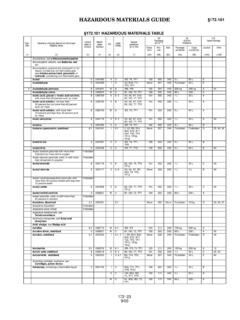
2 AEC Q101 Qualified and PPAP Capable These Devices are Pb free , Halogen free /BFR free and are RoHSCompliantMAXIMUM RATINGS (TA = 25_C, common for NPN and PNP, minussign, , for PNP omitted, unless otherwise noted)RatingSymbolMaxUnitCollector Emitter VoltageVCEO80 VdcEmitter Base VoltageVEB5 VdcCollector Current ContinuousIC8 AdcCollector Current PeakICM16 AdcTotal Power Dissipation @ TC = 25 CDerate above 25 CTotal Power Dissipation (Note 1)@ TA = 25 C Derate above 25 COperating and Storage JunctionTemperature RangeTJ, Tstg 55 to + 150 CESD Human Body ModelHBM3 BVESD Machine ModelMMCVS tresses exceeding those listed in the Maximum Ratings table may damage thedevice.
3 If any of these limits are exceeded, device functionality should not beassumed, damage may occur and reliability may be These ratings are applicable when surface mounted on the minimum padsizes TRANSISTORS8 AMPERES80 VOLTS, 20 WATTSIPAKCASE 369 DSTYLE 1 DPAKCASE 369 CSTYLE 1 MARKING DIAGRAMSA= Assembly LocationY= YearWW= Work WeekJ4xH11= Device Codex = 4 or 5G=Pb free Package1234 AYWWJ4xH11 GSee detailed ordering and shipping information in the packagedimensions section on page 7 of this data INFORMATION1234 AYWWJ4xH11 GIPAKDPAKCOMPLEMENTARY1 BASE3 EMITTERCOLLECTOR2, 41 BASE3 EMITTERCOLLECTOR2, 4 DPAKCASE 369 GSTYLE 11234 MJD44H11 (NPN), MJD45H11 (PNP)
4 CHARACTERISTICSC haracteristicSymbolMaxUnitThermal Resistance, Junction to C/WThermal Resistance, Junction to Ambient (Note 2) C/WLead Temperature for SolderingTL260 C2. These ratings are applicable when surface mounted on the minimum pad sizes CHARACTERISTICS (TA = 25_C, common for NPN and PNP, minus sign, , for PNP omitted, unless otherwise noted)CharacteristicSymbolMinTypMaxUnitO FF CHARACTERISTICSC ollector Emitter Sustaining Voltage(IC = 30 mA, IB = 0)VCEO(sus)80 VdcCollector Cutoff Current(VCE = Rated VCEO, VBE = 0)ICES Cutoff Current(VEB = 5 Vdc)IEBO CHARACTERISTICSC ollector Emitter Saturation Voltage(IC = 8 Adc, IB = Adc)VCE(sat)
5 1 VdcBase Emitter Saturation Voltage(IC = 8 Adc, IB = Adc)VBE(sat) Current Gain(VCE = 1 Vdc, IC = 2 Adc)(VCE = 1 Vdc, IC = 4 Adc)hFE6040 DYNAMIC CHARACTERISTICSC ollector Capacitance(VCB = 10 Vdc, ftest = 1 Mhz)MJD44H11 MJD45H11 Ccb 45130 pFGain Bandwidth Product(IC = Adc, VCE = 10 Vdc, f = 20 Mhz)MJD44H11 MJD45H11fT 8590 MHzSWITCHING TIMESD elay and Rise Times(IC = 5 Adc, IB1 = Adc)MJD44H11 MJD45H11td + tr 300135 nsStorage Time(IC = 5 Adc, IB1 = IB2 = Adc)MJD44H11 MJD45H11ts 500500 nsFall Time(IC = 5 Adc, IB1 = IB2 = Adc)MJD44H11 MJD45H11tf 140100 nsProduct parametric performance is indicated in the Electrical Characteristics for the listed test conditions, unless otherwise noted.
6 Productperformance may not be indicated by the Electrical Characteristics if operated under different (NPN), MJD45H11 (PNP) , TIME (ms) (t), EFFECTIVE TRANSIENT THERMALRqJC(t) = r(t) RqJCRqJC = C/W MAXD CURVES APPLY FOR POWERPULSE TRAIN SHOWNREAD TIME AT t1TJ(pk) - TC = P(pk) qJC(t)P(pk)t1t2 DUTY CYCLE, D = t1 (NORMALIZED) 1. Thermal PULSED = , COLLECTOR CURRENT (AMP)201 VCE, COLLECTOR-EMITTER VOLTAGE (VOLTS) LIMIT @ TC = 25 CWIRE BOND LIMIT57207010100 2. Maximum Forward BiasSafe Operating Area1 ms500 ms5 msThere are two limitations on the Power handling ability ofa transistor: average junction temperature and secondbreakdown.
7 Safe operating area curves indicate IC VCElimits of the transistor that must be observed for reliableoperation; , the transistor must not be subjected to greaterdissipation than the curves data of Figure 2 is based on TJ(pk) = 150_C; TC isvariable depending on conditions. Second breakdown pulselimits are valid for duty cycles to 10% provided TJ(pk) 150_C. TJ(pk) may be calculated from the data inFigure 1. At high case temperatures, thermal limitations willreduce the Power that can be handled to values less than thelimitations imposed by second , TEMPERATURE ( C)050751001251502015105PD, Power DISSIPATION (WATTS) 3.
8 Power DeratingTCTASURFACEMOUNTMJD44H11 (NPN), MJD45H11 (PNP) 4. MJD44H11 DC Current GainFigure 5. MJD45H11 DC Current GainIC, COLLECTOR CURRENT (A) 6. MJD44H11 DC Current GainFigure 7. MJD45H11 DC Current GainFigure 8. MJD44H11 Saturation VoltageVCE(sat)Figure 9. MJD45H11 Saturation VoltageVCE(sat)IC, COLLECTOR CURRENT (A)IC, COLLECTOR CURRENT (A) , DC CURRENT GAINVCE(sat), COLL EMIT SATURATION VOLTAGE (V)150 C 55 C25 CVCE = 1 VIC, COLLECTOR CURRENT (A) , DC CURRENT GAIN150 C 55 C25 CVCE = 1 VIC, COLLECTOR CURRENT (A) , DC CURRENT GAIN150 C 55 C25 CVCE = 4 VIC, COLLECTOR CURRENT (A) , DC CURRENT GAIN150 C 55 C25 CVCE = 4 C 55 C25 CIC/IB = 20IC, COLLECTOR CURRENT (A) (sat), COLL EMIT SATURATION VOLTAGE (V) C 55 C25 CIC/IB = 20 MJD44H11 (NPN), MJD45H11 (PNP) 10.
9 MJD44H11 Saturation VoltageVBE(sat)Figure 11. MJD45H11 Saturation VoltageVBE(sat)IC, COLLECTOR CURRENT (A)IC, COLLECTOR CURRENT (A) 12. MJD44H11 Collector SaturationRegionFigure 13. MJD45H11 Collector SaturationRegionIB, BASE CURRENT (mA)IB, BASE CURRENT (mA)10, 14. MJD44H11 CapacitanceFigure 15. MJD45H11 CapacitanceVR, REVERSE VOLTAGE (V) (sat), BASE EMIT SATURATIONVOLTAGE (V)VCE, COLLECTOR EMITTER VOLTAGE (V)C, CAPACITANCE (pF)150 C 55 C25 CIC/IB = (sat), BASE EMIT SATURATIONVOLTAGE (V)150 C 55 C25 CIC/IB = = 25 CIC = 8 A1 AIC = 3 AIC = A10, , COLLECTOR EMITTER VOLTAGE (V) = 25 CCobVR, REVERSE VOLTAGE (V) , CAPACITANCE (pF)CobIC = 8 A1 AIC = 3 AIC = AMJD44H11 (NPN), MJD45H11 (PNP) 16.
10 MJD44H11 Current Gain Bandwidth ProductFigure 17. MJD45H11 Current Gain Bandwidth ProductIC, COLLECTOR CURRENT (A)IC, COLLECTOR CURRENT (A) u, CURRENT GAIN BANDWIDTHPRODUCTfTa u, CURRENT GAIN BANDWIDTHPRODUCTVCE = 2 VVCE = 2 VMJD44H11 (NPN), MJD45H11 (PNP) INFORMATIOND evicePackage TypePackageShipping MJD44H11 GDPAK(Pb free )369C75 Units / RailNJVMJD44H11 GDPAK(Pb free )369C75 Units / RailMJD44H11 1 GDPAK 3(Pb free )369D75 Units / RailMJD44H11 RLGDPAK(Pb free )369C1,800 / Tape & ReelNJVMJD44H11 RLG*DPAK(Pb free )369C1,800 / Tape & ReelMJD44H11T4 GDPAK(Pb free )