Example: biology
MOSFET transistor I-V characteristics
Lecture 20-8 PMOSFETs • All of the voltages are negative • Carrier mobility is about half of what it is for n channels p+ n S G D B p+ • The bulk is now connected to the most positive potential in the circuit • Strong inversion occurs when the channel becomes as p-type as it was n-type • The inversion layer is a positive charge that is sourced by the larger potential
Tags:
Information
Domain:
Source:
Link to this page:
Documents from same domain
Computer Architecture: Dataflow (Part I)
course.ece.cmu.eduComputer Architecture,” ACM Computing Surveys 1982. ! Veen, “Dataflow Machine Architecture,” ACM Computing Surveys 1986. ! Gurd et al., “The Manchester prototype dataflow computer,” CACM 1985. ! Arvind and Nikhil, “Executing a Program on the MIT Tagged-Token Dataflow Architecture,” IEEE TC 1990. !

Computer Architecture: Vector Processing: SIMD/Vector/GPU ...
course.ece.cmu.eduCarnegie Mellon University Vector Processing: Exploiting Regular (Data) Parallelism Data Parallelism Concurrency arises from performing the same operations on different pieces of data Single instruction multiple data (SIMD) E.g., dot product of two vectors Contrast with data flow

Computer Architecture: Branch Prediction
course.ece.cmu.eduHow to Handle Control Dependences Critical to keep the pipeline full with correct sequence of dynamic instructions. Potential solutions if the instruction is a control-flow instruction: Stall the pipeline until we know the next fetch address Guess the next fetch address (branch prediction) Employ delayed branching (branch delay slot) Do something else (fine-grained multithreading)

Computer Architecture: Main Memory (Part I)
course.ece.cmu.eduMemory Bank Organization and Operation Read access sequence: 1. Decode row address & drive word-lines 2. Selected bits drive bit-lines • Entire row read 3. Amplify row data 4. Decode column address & select subset of row • Send to output 5. …

CMOS Power Consumption - ECE:Course Page
course.ece.cmu.eduWays to reducing power consumption Load capacitance (C L) ⌧Roughly proportional to the chip area Switching activity (avg. number of transitions/cycle) ⌧Very data dependent ⌧A big portion due to glitches (real-delay) Clock frequency (f) ⌧Lowering only f decreases average power, but total energy is the same and throughput is worse 1.00 1 ...

HDL Compiler for Verilog Reference Manual
course.ece.cmu.eduComments? E-mail your comments about Synopsys documentation to doc@synopsys.com HDL Compiler for Verilog Reference Manual Version 2000.05, May 2000

Computer Architecture: Multithreading
course.ece.cmu.eduSun Niagara Multithreaded Pipeline 13 Tera MTA Fine-grained Multithreading 256 processors, each with a 21-cycle pipeline 128 active threads A thread can issue instructions every 21 cycles Then, why 128 threads? Memory latency: approximately 150 cycles No data cache Threads can be blocked waiting for memory More threads better ability to tolerate memory latency

A Primer on Memory Consistency and Cache Coherence
course.ece.cmu.eduDaniel J. Sorin, Duke University Mark D. Hill and David A. Wood, University of Wisconsin, Madison ... We thank Blake Hechtman for implementing and testing (and debugging!) all of the coherence protocols in this primer. As the reader will soon …
Related documents

LTC4441/LTC4441-1 - N-Channel MOSFET Gate Driver
www.analog.comLTC4441/LTC4441-1 1 44411fa Typical applicaTion FeaTures DescripTion N-Channel MOSFET Gate Driver The LTC®4441/LTC4441-1 is an N-channel MOSFET gate driver that can supply up to 6A of peak output current.

NTD2955, NVD2955 MOSFET – Power, P-Channel, DPAK
www.onsemi.comNTD2955/D NTD2955, NVD2955 MOSFET – Power, P-Channel, DPAK-60 V, -12 A This Power MOSFET is designed to withstand high energy in the avalanche and commutation modes. Designed for low−voltage, high− speed switching applications in power supplies, converters, and power motor controls. These devices are particularly well suited for bridge
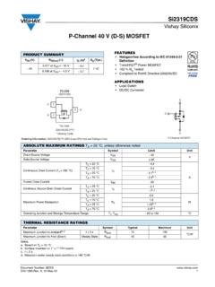
P-Channel 40 V (D-S) MOSFET - Vishay Intertechnology
www.vishay.comP-Channel 40 V (D-S) MOSFET FEATURES • Halogen-free According to IEC 61249-2-21 Definition TEFhcne †Tr ® Power MOSFET † 100 % Rg Tested † Compliant to RoHS Directive 2002/95/EC APPLICATIONS † Load Switch † DC/DC Converter Notes: a. Based on TC = 25 °C. b. Surface mounted on 1" x 1" FR4 board. c. t = 5 s. d.
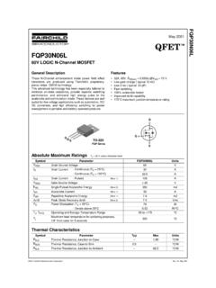
FQP30N06L 60V LOGIC N-Channel MOSFET - SparkFun …
cdn.sparkfun.com60V LOGIC N-Channel MOSFET General Description ... VDSS Drain-Source Voltage 60 V ID Drain Current - Continuous (TC = 25°C) 32 A - Continuous ... 7.9 mJ dv/dt Peak Diode Recovery dv/dt (Note 3) 7.0 V/ns PD Power Dissipation (TC = 25°C) 79 W - Derate above 25°C 0.53 W/°C TJ, TSTG Operating and Storage Temperature Range -55 to +175 °C TL
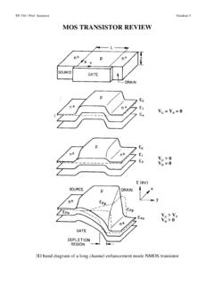
MOS TRANSISTOR REVIEW - Stanford University
web.stanford.eduec ≈ 5 × 10⁴ V/cm for holes, hence velocity saturation for P-channel MOSFET will not become important until L < 0.25 µm. Figure. Effects of velocity saturation on the MOSFET I-V characteristics. (a)Experimental characteristics of a MOSFET with L = 2.7 µm, x0 =0.05 µm,
P-Channel 80-V (D-S) MOSFET - Vishay Intertechnology
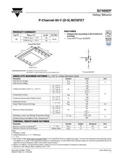
www.vishay.comP-Channel 80-V (D-S) MOSFET ... 60 80 100 25 50 75 100 125 150 T C - Case Temperature (°C) Power (W) www.vishay.com 6 Document Number: 73438 S09-0271-Rev. C, 16-Feb-09 Vishay Siliconix Si7469DP TYPICAL CHARACTERISTICS 25 °C, unless otherwise noted Vishay Siliconix maintains worldwide manufacturing capability. Products may be manufactured at ...

NX7002AK - Nexperia
assets.nexperia.com60 V, single N-channel Trench MOSFET All information provided in this document is subject to legal disclaimers. Product data sheet 6 August 2015 2 / 16 5. Pinning information Table 2. Pinning information Pin Symbol Description Simplified outline Graphic symbol 1 G gate 2 S source 3 D drain 1 2 3 TO-236AB (SOT23) 017aaa255 G D S 6. Ordering ...
NDS7002A - N-Channel Enhancement Mode Field Effect …
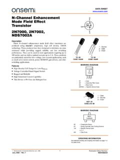
www.onsemi.com2N7000, 2N7002, NDS7002A www.onsemi.com 2 ABSOLUTE MAXIMUM RATINGS Values are at TC = 25°C unless otherwise noted. Symbol Parameter Value 2N7000 2N7002 NDS7002A Unit VDSS Drain−to−Source Voltage 60 V VDGR Drain−Gate Voltage (RGS ≤ 1 MW) 60 V VGSS Gate−Source Voltage − Continuous ±20 V Gate−Source Voltage − Non Repetitive (tp < 50 ms) …