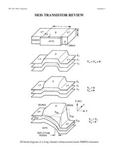
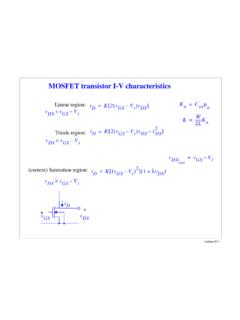
Transcription of NX7002AK - Nexperia
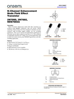
1 NX7002AK60 V, single N- channel Trench MOSFET6 August 2015 Product data sheet1. General descriptionN- channel enhancement mode Field-Effect Transistor (FET) in a small SOT23(TO-236AB) Surface-Mounted Device (SMD) plastic package using Trench Features and benefits Very fast switching Trench MOSFET technology ESD protected3. Applications Relay driver High-speed line driver Low-side loadswitch Switching circuits4. Quick reference dataTable 1. Quick reference dataSymbolParameterConditionsMinTypMaxUn itVDSdrain-source voltage--60 VVGS gate-source voltageTj = 25 C-20-20 VVGS = 10 V; Tsp = 25 C--300mAIDdrain currentVGS = 10 V; Tamb = 25 C[1]--190mAStatic characteristicsRDSondrain-source on-stateresistanceVGS = 10 V; ID = 100 mA; Tj = 25 [1]Device mounted on an FR4 PCB, single-sided copper, tin-plated, mounting pad for drain 1 cm2.
2 Nexperia 2017. All rights reservedNexperiaNX7002AK60 V, single N- channel Trench MOSFETNX7002 AKAll information provided in this document is subject to legal data sheet6 August 20152 / 165. Pinning informationTable 2. Pinning informationPinSymbolDescriptionSimplifie d outlineGraphic symbol1 Ggate2 Ssource3 Ddrain123TO-236AB (SOT23)017aaa255 GDS6. Ordering informationTable 3. Ordering informationPackageType numberNameDescriptionVersionNX7002 AKTO-236 ABplastic surface-mounted package; 3 leadsSOT237. MarkingTable 4. Marking codesType numberMarking code[1] NX7002AK %CM[1] % = placeholder for manufacturing site code Nexperia 2017. All rights reservedNexperiaNX7002AK60 V, single N- channel Trench MOSFETNX7002 AKAll information provided in this document is subject to legal data sheet6 August 20153 / 168.
3 Limiting valuesTable 5. Limiting valuesIn accordance with the Absolute Maximum Rating System (IEC 60134).SymbolParameterConditionsMinMaxUn itVDSdrain-source voltage-60 VVGS gate-source voltageTj = 25 C-2020 VVGS = 10 V; Tsp = 25 C-300mAVGS = 10 V; Tamb = 25 C[1]-190mAIDdrain currentVGS = 10 V; Tamb = 100 C[1]-120mAIDM peak drain currentTamb = 25 C; single pulse; tp 10 s-760mA[2]-265mWTamb = 25 C[1]-325mWPtottotal power dissipationTsp = 25 C-1330mWTjjunction temperature-55150 CTambambient temperature-55150 CTstgstorage temperature-65150 CSource-drain diodeISsource currentTamb = 25 C[1]-190mA[1]Device mounted on an FR4 PCB, single-sided copper, tin-plated, mounting pad for drain 1 cm2.[2] Device mounted on an FR4 Printed-Circuit Board (PCB), single-sided copper, tin-plated and ( C)-751751252575-25017aaa1234080120 Pder(%)0 Fig.
4 1. Normalized total power dissipation as afunction of junction temperatureTj( C)-751751252575-25017aaa1244080120 Ider(%)0 Fig. 2. Normalized continuous drain current as afunction of junction temperature Nexperia 2017. All rights reservedNexperiaNX7002AK60 V, single N- channel Trench MOSFETNX7002 AKAll information provided in this document is subject to legal data sheet6 August 20154 / 16017aaa466 VDS (V)10-110210110-110-21ID(A)10-3 Limit RDSon = VDS/ID(1)(2)(3)(4)(5)(6)IDM = single pulse(1) tp = 100 s(2) tp = 1 ms(3) tp = 10 ms(4) DC; Tsp = 25 C(5) tp = 100 ms(6) DC; Tamb = 25 C; drain mounting pad 1 cm2 Fig. 3. Safe operating area; junction to ambient; continuous and peak drain currents as a function of drain-source voltage9. Thermal characteristicsTable 6. Thermal characteristicsSymbolParameterConditions MinTypMaxUnit[1]-410470K/WRth(j-a)therma l resistancefrom junction toambientin free air[2]-330380K/WRth(j-sp)thermal resistancefrom junction to solderpoint--95K/W[1] Device mounted on an FR4 PCB, single-sided copper, tin-plated and standard footprint.
5 [2]Device mounted on an FR4 PCB, single-sided copper, tin-plated, mounting pad for drain 1 cm2. Nexperia 2017. All rights reservedNexperiaNX7002AK60 V, single N- channel Trench MOSFETNX7002 AKAll information provided in this document is subject to legal data sheet6 August 20155 / 16017aaa467101102103 Zth(j-a)(K/W)10-110-51010-210-410210-1tp (s)10-31031duty cycle = PCB, standard footprintFig. 4. Transient thermal impedance from junction to ambient as a function of pulse duration; typical values017aaa468101102103 Zth(j-a)(K/W)10-110-51010-210-410210-1tp (s)10-31031duty cycle = PCB, mounting pad for drain 1 cm2 Fig. 5. Transient thermal impedance from junction to ambient as a function of pulse duration; typical values Nexperia 2017. All rights reservedNexperiaNX7002AK60 V, single N- channel Trench MOSFETNX7002 AKAll information provided in this document is subject to legal data sheet6 August 20156 / 1610.
6 CharacteristicsTable 7. CharacteristicsSymbolParameterConditions MinTypMaxUnitStatic characteristicsV(BR)DSSdrain-sourcebreak down voltageID = 250 A; VGS = 0 V; Tj = 25 C60--VVGS thgate-source thresholdvoltageID = 250 A; VDS = VGS; Tj = 25 = 60 v ; VGS = 0 V; Tj = 25 C--1 AIDSS drain leakage currentVDS = 60 v ; VGS = 0 V; Tj = 150 C--10 AVGS = 20 V; VDS = 0 V; Tj = 25 C--2 AVGS = -20 V; VDS = 0 V; Tj = 25 C---2 AVGS = 10 V; VDS = 0 V; Tj = 25 AVGS = -10 V; VDS = 0 V; Tj = 25 AVGS = 5 V; VDS = 0 V; Tj = 25 C--100nAIGSS gate leakage currentVGS = -5 V; VDS = 0 V; Tj = 25 C---100nAVGS = 10 V; ID = 100 mA; Tj = 25 VGS = 10 V; ID = 100 mA; Tj = 150 RDSondrain-source on-stateresistanceVGS = 5 V; ID = 100 mA; Tj = 25 gfsforwardtransconductanceVDS = 10 V; ID = 200 mA.
7 Tj = 25 C-500-mSDynamic characteristicsQG(tot)total gate chargeVDS = 30 V; ID = 200 mA; VGS = V;Tj = 25 capacitance-1520pFCossoutput transfercapacitanceVDS = 10 V; f = 1 MHz; VGS = 0 V;Tj = 25 C-2-pFtd(on)turn-on delay time-612nstrrise time-7-nstd(off)turn-off delay time-1120nstffall timeVDS = 40 V; RL = 250 ; VGS = 10 V;RG(ext) = 6 ; Tj = 25 C-5-nsSource-drain diodeVSDsource-drain voltageIS = 115 mA; VGS = 0 V; Tj = 25 Nexperia 2017. All rights reservedNexperiaNX7002AK60 V, single N- channel Trench MOSFETNX7002 AKAll information provided in this document is subject to legal data sheet6 August 20157 / 16 VDS (V) (A) = = 25 CFig. 6. Output characteristics: drain current as afunction of drain-source voltage; typical values017aaa470 VGS (V)032110-410-510-3ID(A)10-6(1)(2)(3)Tj = 25 C; VDS = 5 V(1) minimum values(2) typical values(3) maximum valuesFig.
8 7. Sub-threshold drain current as a function ofgate-source voltageID (A) ( ) = 25 CFig. 8. Drain-source on-state resistance as a functionof drain current; typical valuesVGS (V)0108462017aaa4724812 RDSon0(1)(2)ID = A(1) Tj = 150 C(2) Tj = 25 CFig. 9. Drain-source on-state resistance as a functionof gate-source voltage; typical values Nexperia 2017. All rights reservedNexperiaNX7002AK60 V, single N- channel Trench MOSFETNX7002 AKAll information provided in this document is subject to legal data sheet6 August 20158 / 16 VGS (V) (A)0(1)(2)VDS > ID RDSon(1) Tj = 25 C(2) Tj = 150 CFig. 10. Transfer characteristics: drain current as afunction of gate-source voltage; typical valuesTj ( C) 11. Normalized drain-source on-state resistanceas a function of junction temperature; typicalvaluesTj ( C) (th)(V)0(1)(2)(3)ID = mA; VDS = VGS(1) maximum values(2) typical values(3) minimum valuesFig.
9 12. Gate-source threshold voltage as a function ofjunction temperatureVDS (V)10-1102101017aaa476101102C(pF)10-1(1) (2)(3)f = 1 MHz; VGS = 0 V(1) Ciss(2) Coss(3) CrssFig. 13. Input, output and reverse transfer capacitancesas a function of drain-source voltage; typicalvalues Nexperia 2017. All rights reservedNexperiaNX7002AK60 V, single N- channel Trench MOSFETNX7002 AKAll information provided in this document is subject to legal data sheet6 August 20159 / 16QG (nC) (V)0ID = A; VDS = 30 V; Tamb = 25 CFig. 14. Gate-source voltage as a function of gatecharge; typical values017aaa137 VGSVGS(th)QGS1 QGS2 QGDVDSQG(tot)IDQGSVGS(pl)Fig. 15. MOSFET transistor: Gate charge waveformdefinitions017aaa478 VSD (V) (A)0(1)(2)VGS = 0 V(1) Tj = 150 C(2) Tj = 25 CFig. 16. Source current as a function of source-drain voltage; typical values Nexperia 2017.
10 All rights reservedNexperiaNX7002AK60 V, single N- channel Trench MOSFETNX7002 AKAll information provided in this document is subject to legal data sheet6 August 201510 / 1611. Test informationt1t2Pt006aaa812dutycycle =t1t2 Fig. 17. Duty cycle definition Nexperia 2017. All rights reservedNexperiaNX7002AK60 V, single N- channel Trench MOSFETNX7002 AKAll information provided in this document is subject to legal data sheet6 August 201511 / 1612. Package outlineReferencesOutlineversionEuropeanp rojectionIssue dateIECJEDECJEITASOT23TO-236 ABsot023_po14-06-1914-09-22 Plastic surface-mounted package; 3 leadsSOT23bpDAA1 LpQHEE012 (mm are the original dimensions) XFig. 18. Package outline TO-236AB (SOT23) Nexperia 2017. All rights reservedNexperiaNX7002AK60 V, single N- channel Trench MOSFETNX7002 AKAll information provided in this document is subject to legal data sheet6 August 201512 / 1613.