Transcription of NE5534 - Operational Amplifier, Low Noise, Single
1 Semiconductor Components Industries, LLC, 2012 July, 2012 Rev. 31 Publication Order Number: NE5534 /DNE5534, SA5534, SE5534,NE5534A, SA5534A,SE5534 AOperational Amplifier, Low Noise, SingleThe NE/SA/SE5534/5534A are Single high-performance low noise Operational amplifiers. Compared to other Operational amplifiers, such as TL083, they show better noise performance, improved output drive capability, and considerably higher small-signal and power makes the devices especially suitable for application in high quality and professional audio equipment, in instrumentation and control circuits and telephone channel amplifiers. The op amps are internally compensated for gain equal to, or higher than, three.
2 The frequency response can be optimized with an external compensation capacitor for various applications (unity gain amplifier, capacitive load, slew rate, low overshoot, etc.).Features Small-Signal Bandwidth: 10 MHz Output Drive Capability: 600 W, 10 VRMS at VS = "18 V Input Noise Voltage: 4nV Hz DC Voltage Gain: 100000 AC Voltage Gain: 6000 at 10 kHz power Bandwidth: 200 kHz Slew Rate: 13 V/ms Large supply Voltage Range: " to "20 V Pb Free Packages are AvailableApplications Audio Equipment Instrumentation and Control Circuits Telephone Channel Amplifiers Medical detailed ordering and shipping information in the packagedimensions section on page 8 of this data INFORMATIONPIN CONNECTIONSSOIC 8D SUFFIXCASE 751 Top ViewPDIP 8N SUFFIXCASE 6261887654321 BALANCE/COMPENSATIONV+OUTPUTCOMPENSATION BALANCEINVERTING INPUTNON-INVERTINGV D, N Packages18 See general marking information in the device markingsection on page 8 of this data MARKING INFORMATIONNE5534, SA5534, SE5534, NE5534A, SA5534A, SE5534 1.
3 Equivalent SchematicMAXIMUM RATINGSR atingSymbolValueUnitSupply VoltageVS"22 VInput VoltageVIN"V SupplyVDifferential Input Voltage (Note 1)VDIFF" Temperature RangeNESASETamb0 to +70 40 to +85 55 to +125 CStorage Temperature RangeTstg 65 to +150 CJunction TemperatureTj150 CPower Dissipation at 25 CN PackageD PackagePD1150750mWThermal Resistance, Junction to AmbientN PackageD PackageRqJA130158 C/WOutput Short-Circuit Duration (Note 2) Indefinite Lead Soldering Temperature (10 sec max)Tsld230 CStresses exceeding Maximum Ratings may damage the device. Maximum Ratings are stress ratings only. Functional operation above theRecommended Operating Conditions is not implied. Extended exposure to stresses above the Recommended Operating Conditions may affectdevice Diodes protect the inputs against overvoltage.
4 Therefore, unless current-limiting resistors are used, large currents will flow if the differential inputvoltage exceeds V. Maximum current should be limited to "10 Output may be shorted to ground at VS = "15 V, Tamb = 25 C. Temperature and/or supply voltages must be limited to ensure dissipation ratingis not , SA5534, SE5534, NE5534A, SA5534A, SE5534 ELECTRICAL CHARACTERISTICS (Tamb = 25 C; VS = "15 V, unless otherwise noted.) (Notes 3, 4 and 5)CharacteristicSymbolTest ConditionsNE/SA5534/5534 ASE5534/5534 AUnitMinTypMaxMinTypMaxVOS VoltageOvertemperature mV/ CIOS 20300 10200nAOffset CurrentOvertemperature 400 500nADIOS/DT 200 200 pA/ CIB 5001500 400800nAInput CurrentOvertemperature 2000 1500nADIB/DT nA/ CSupply CurrentPer Op AmpICCO vertemperature Mode Input RangeVCM"12"13 "12"13 VCommon Mode rejection RatioCMRR70100 80100 dBPower supply rejection RatioPSRR 10100 1050mV/VLarge-Signal Voltage GainAVOLRL 600 W,VO = "10 VOvertemperature2515100 5025100 V/mVOutput SwingVOUTRL w 600 W"12"13 "12"13 VOvertemperature"10"12 "10"12 RL w 600 W.
5 VS = "18 V"15"16 "1516 RL w kW"13" "13" Overtemperature"12" "12" Input ResistanceRIN30100 50100 kWOutput Short Circuit CurrentISC 38 38 mA3. For NE5534 /5534A, TMIN = 0 C, TMAX = 70 For SA5534/5534A, TMIN = 40 C, TMAX = +85 For SE5534/5534A, TMIN = 55 C, TMAX = +125 , SA5534, SE5534, NE5534A, SA5534A, SE5534 ELECTRICAL CHARACTERISTICS (Tamb = 25 C; VS = "15 V, unless otherwise noted.)CharacteristicSymbolTest ConditionsNE/SA5534/5534 ASE5534/5534 AUnitMinTypMaxMinTypMaxOutput ResistanceROUTAV = 30 dBclosed-loop f = 10 kHz;RL = 600 W;CC = 22 pF WTransient ResponseVoltage-follower,VIN = 50 mV RL = 600 W,CC = 22 pF,CL = 100 pFRise TimetR 20 20 nsOvershoot 20 20 %Transient ResponseVIN = 50 mV,RL = 600 W,CC = 47 pF,CL = 500 pFRise TimetR 50 50 nsOvershoot 35 35 %GainAVf = 10 kHz, CC = 0 V/mVf = 10 kHz,CC = 22 pF Gain Bandwidth ProductGBWCC = 22 pF,CL = 100 pF 10 10 MHzSlew RateSRCC = 0 13 13 V/msCC = 22 pF power Bandwidth VOUT = "10 V,CC = 0 pF 200 200 kHzVOUT = "10 V,CC = 22 pF 95 95 VOUT = "14 V,RL = 600 W,CC = 22 pF,VCC = "18 V 70 70 ELECTRICAL CHARACTERISTICS (Tamb = 25 C; VS = 15 V, unless otherwise noted.)
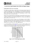
6 CharacteristicSymbolTest ConditionsNE/SA/SE5534NE/SA/SE5534 AUnitMinTypMaxMinTypMaxInput Noise VoltageVNOISEfO = 30 HzfO = kHz HzInput Noise CurrentINOISEfO = 30 HzfO = kHz pA/ HzBroadband Noise Figure f = 10 Hz to20 kHz;RS = kW dBChannel Separation f = kHz;RS = kW 110 110 dBNE5534, SA5534, SE5534, NE5534A, SA5534A, SE5534 PERFORMANCE CHARACTERISTICSGAIN (dB)(nV Hz )1010210310410510610712080400-40f (Hz)161284004080102103104105106107403020 100806040200-55-250255075100+125-55-2502 55075100 +1251,41,20,80,4030201000102001020024610 210110 110 210102103104CC(pF)f (Hz)f (Hz)Tamb (oC)Tamb (oC)TYPTYPTYPTYPTYPNEGPOSCC =0pF22pF47pFCC = 0CC = 22pFS(V/ms)(V)Vo(p-p)IO(mA)II(mA)VIN (V)IPIN(mA)Vp; -VN (V)Vp; -VN (V)Figure 2.
7 Open-LoopFrequency ResponseFigure 3. Slew Rate as aFunction of CompensationCapacitanceGAIN (dB)6040200-20103104105106107108f (Hz)CC = 0; RF = 10kW; RE = 100 WCC = 0; RF = 9kW; RE = 1kWCC = 22pF; RF = 1kW; RE = Figure 4. Closed LoopFrequency ResponseFigure 5. Large SignalFrequency ResponseFigure 6. OutputShort Circuit CurrentFigure 7. Input BiasCurrentFigure 8. Input Common ModeVoltage RangeFigure 9. supply CurrentPer Op AmpFigure 10. Input NoiseVoltage DensityTYPICAL VALUES58 CCVS = +15 VTYPICAL VALUESVS = +15 VTYPICAL VALUESVS = +15 VVS = +15 VTYPICAL VALUESIO = 0NE5534, SA5534, SE5534, NE5534A, SA5534A, SE5534 PERFORMANCE CHARACTERISTICSRS (W)(pA Hz )(nV Hz )10210110 110 210102103104f (Hz)TYPF igure 11.
8 Input NoiseCurrent Density10102103104105106 Figure 12. Total InputNoise Density01020RS (W)Figure 13. Broadband InputNoise VoltageVn(rms)In(rms)1061051041031021011 0 110 2Vn(rms)(mV)10210110 110 210Hz1kHzTHERMAL NOISEOF SOURCE RESISTANCE10Hz TO 20kHz200Hz TO 4kHzTYPICAL VALUESTYPICAL VALUESNE5534, SA5534, SE5534, NE5534A, SA5534A, SE5534 LOAD CIRCUITSCCRSREVI100kW22kW600W25 WRF18576432-++-23856100pFV+V-Figure 14. Frequency Compensation andOffset Voltage Adjustment CircuitFigure 15. Closed-Loop Frequency Response55345534CC(nV Hz )(nV Hz )CALOSCPOWERSUPPLYCALMETER+VCC-VCC+40dB1 0kW100 WTEST BOARDGND1 WDUT+-BANDPASSAT 1kHzBANDPASSAT 30 HzFigure 16. Noise Test Block DiagramNE5534, SA5534, SE5534, NE5534A, SA5534A, SE5534 8N SUFFIXCASE 626 SOIC 8D SUFFIXCASE 751x= Blank or AA= Assembly LocationWL, L= Wafer LotYY, Y= YearWW, W = Work WeekG or G= Pb Free PackageMARKING DIAGRAMSN5234 ALYWA G18S5234 ALYWA G18S5234 ALYW G18NE5234xNAWLYYWWGSE5234xNAWLYYWWGORDER ING INFORMATIOND eviceDescriptionTemperature RangeShipping NE5534AD8 Pin Plastic Small Outline (SO 8) Package0 to +70 C98 Units / RailNE5534 ADG8 Pin Plastic Small Outline (SO 8) Package (Pb Free)0 to +70 C98 Units / RailNE5534 ADR28 Pin Plastic Small Outline (SO 8) Package0 to +70 C2500 / Tape & ReelNE5534 ADR2G8 Pin Plastic Small Outline (SO 8)
9 Package (Pb Free)0 to +70 C2500 / Tape & ReelNE5534AN8 Pin Plastic Dual In Line Package (PDIP 8)0 to +70 C50 Units / RailNE5534 ANG8 Pin Plastic Dual In Line Package (PDIP 8) (Pb Free)0 to +70 C50 Units / RailNE5534D8 Pin Plastic Small Outline (SO 8) Package0 to +70 C98 Units / RailNE5534DG8 Pin Plastic Small Outline (SO 8) Package (Pb Free)0 to +70 C98 Units / RailNE5534DR28 Pin Plastic Small Outline (SO 8) Package0 to +70 C2500 / Tape & ReelNE5534DR2G8 Pin Plastic Small Outline (SO 8) Package (Pb Free)0 to +70 C2500 / Tape & ReelNE5534N8 Pin Plastic Dual In Line Package (PDIP 8)0 to +70 C50 Units / RailNE5534NG8 Pin Plastic Dual In Line Package (PDIP 8) (Pb Free)0 to +70 C50 Units / RailSA5534AD8 Pin Plastic Small Outline (SO 8) Package 40 to +85 C98 Units / RailSA5534 ADG8 Pin Plastic Small Outline (SO 8) Package (Pb Free) 40 to +85 C98 Units / RailSA5534 ADR28 Pin Plastic Small Outline (SO 8) Package 40 to +85 C2500 / Tape & ReelSA5534 ADR2G8 Pin Plastic Small Outline (SO 8) Package (Pb Free) 40 to +85 C2500 / Tape & ReelSA5534AN8 Pin Plastic Dual In Line Package (PDIP 8) 40 to +85 C50 Units / RailSA5534 ANG8 Pin Plastic Dual In Line Package (PDIP 8) (Pb Free) 40 to +85 C50 Units / RailSA5534N8 Pin Plastic Dual In Line Package (PDIP 8) 40 to +85 C50 Units / RailSA5534NG8 Pin Plastic Dual In Line Package (PDIP 8) (Pb Free)
10 40 to +85 C50 Units / RailSE5534AN8 Pin Plastic Dual In Line Package (PDIP 8) 55 to +125 C50 Units / RailSE5534 ANG8 Pin Plastic Dual In Line Package (PDIP 8) (Pb Free) 55 to +125 C50 Units / RailSE5534N8 Pin Plastic Dual In Line Package (PDIP 8) 55 to +125 C50 Units / RailSE5534NG8 Pin Plastic Dual In Line Package (PDIP 8) (Pb Free) 55 to +125 C50 Units / Rail For information on tape and reel specifications, including part orientation and tape sizes, please refer to our Tape and Reel Packaging SpecificationBrochure, BRD8011 8 CASE 626 05 ISSUE PDATE 22 APR 2015 SCALE 1:11458b2 NOTE 8 DbLA1 AeBXXXXXXXXXAWLYYWWGEGENERICMARKING DIAGRAM*XXXX= Specific Device CodeA= Assembly LocationWL= Wafer LotYY= YearWW= Work WeekG= Pb Free Package*This information is generic.