Transcription of NTE195A Silicon NPN Transistor RF Power …
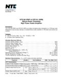
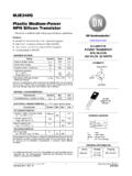
1 NTE195 ASilicon NPN TransistorRF Power Amp/Driver, CBDescription:The NTE195A is designed primarily for use in large signal output amplifier stages. Intended for usein Citizen Band communications equipment operating to 30 MHz. High breakdown voltages allow ahigh percentage of up modulation in AM :DSpecified , 28 MHz Characteristic: Power Output = Gain= 10dBEfficiency= 70% TypicalAbsolute Maximum Ratings:Collector Emitter Voltage, VCER 70V.. Collector Base Voltage, VCBO 70V.. Emitter Base Voltage, VEBO .. Collector Current Continuous, IC .. Total Device Dissipation (TC = +25 C), PD 8W.
2 Derate above 25 C.. Storage Temperature Range, Tstg 65 to +200 C.. Electrical Characteristics: (TA = +25 C, unless otherwise specified)ParameterSymbolTest ConditionsMinTypMaxUnitOFF CharacteristicsCollector Emitter Breakdown VoltageV(BR)CESIC = 200mA, VBE = 070 VEmitter Base Breakdown VoltageV(BR)EBOIE = 1mA, IC = 04 VCollector Cutoff CurrentICBOVCB = 15V, IE = 0 CharacteristicsDC Current GainhFEVCE = 2V, IC = 400mA30 Dynamic CharacteristicsCapacitanceCobVCB = , IE = 0, f = 1 MHz 3570pFElectrical Characteristics (Cont d): (TA = +25 C, unless otherwise specified)ParameterSymbolTest ConditionsMinTypMaxUnitFunctional TestCommon Emitter Amplifier Power GainGPEPOUT = , VCC = , f = 27 MHz10 dBCollector Efficiency POUT = , VCC = , f = 27 MHz,Note %Percent Up Modulation f = 27 MHz, Note 2 85 %Parallel Equivalent Input ResistanceRinPOUT = , VCC = , f = 27 MHz 21 Parallel Equivalent Input CapacitanceCinPOUT = , VCC = , f = 27 MHz 900 pFParallel Equivalent Output CapaciatnceCoutPOUT = , VCC = , f = 27 MHz 200 pFNote 1.
3 = RF POUT 100(VCC) (IC)Note 2. Percentage Up Modulation is measured by setting the Carrier Power (PC) to Watts withVCC = and noting the Power input. The peak envelope Power (PEP) is noted afterdoubling the original Power input to simulate driver modulation (at a 25% duty cycle for ther-mal considerations) and raising the VCC to 25 Vdc (to simulate the modulating voltage). Per-centage Up Modulation is then determined by the relation:Percentage Up Modulation = (PEP) 1/2 1 ( ) ( ) ( ) Dia ( ) Dia Max45 .031 (.793) ( )