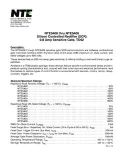
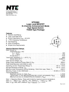
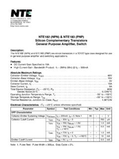
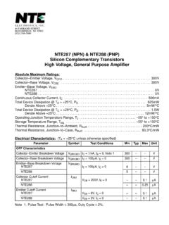
Transcription of NTE966 Integrated Circuit Terminal Positive Voltage ...
1 NTE966 Integrated Circuit3 Terminal Positive Voltage Regulator, 12 VThe NTE966 fixed Voltage regulator is a monolithic Integrated Circuit in a TO220 type package de-signed for use in a wide variety of applications including local, on card regulation. This regulator em-ploys internal current limiting, thermal shutdown, and safe area compensation. With adequate heat-sinking it can deliver output currents in excess of :DOutput Current in Excess of AmpereDNo External Components ReguiredDInternal Thermal Overload ProtectionDInternal Short Circuit Current LimitingDOutput Transistor Safe Area CompensationAbsolute Maximum Ratings: (TA = +25 C unless otherwise specified)Input Voltage , Vin35 Vdc.. Power Dissipation (TA = +25 C), PDInternally Limited.
2 Derate above +25 C.. Power Dissipation (TC = +25 C), PDInternally Limited.. Derate above +75 C200mW/ C.. Thermal Resistance, Junction to Ambient, RthJA65 C/W.. Thermal Resistance, Junction to Case, RthJC5 C/W.. Operating Junction Temperature Range, TJ 55 to +150 C.. Storage Junction Temperature Range, Tstg 65 to +150 C.. Electrical Characteristics: (Vin = 19V, IO = 500mA, TJ = 0 to +125 C unless otherwise specified)ParameterSymbolTest ConditionsMinTypMaxUnitOutput VoltageVOTJ = +25 IO 1A, PO 15W, Vin RegulationReglineTJ = +25 C, Note Vin 20V 13240mV16V Vin 22V 6120mVLoad RegulationRegloadTJ = +25 C, Note 15mA IO 45160mV250mA IO 750mA 1680mVNote 1. Load and line regulation are specified at constant junction temperature.
3 Changes in VO dueto heating effects must be taken into account separately. Pulse testing with low duty cycleis Characteristics (Cont d):(Vin = 19V, IO = 500mA, TJ = 0 to +125 C unless otherwisespecified)ParameterSymbolTest ConditionsMinTypMaxUnitQuiescent CurrentIBTJ = +25 C Current Change Vin 30V IO 1A RejectionRR15V Vin 25V, f = 120Hz 60 dBDropout VoltageVin VOTJ = +25 C, IO = 1A 2 VOutput Noise VoltageVnTA = +25 C, 10Hz f 100kHz 10 V/VOOutput ResistancerOf = 1kHz 18 m Short Circuit Current LimitIscTA = +25 C, Vin = 35V APeak Output CurrentImaxTJ = +25 C AAverage Temperature Coefficientof Output VoltageTCVO mV/ CApplication Information:The NTE966 fixed Voltage regulator is designed with Thermal Overload Protection that shuts downthe Circuit when subjected to an excessive power overload condition, Internal Short Circuit Protectionthat limits the maximum current the Circuit will pass, and Output Transistor Safe Area Compensationthat reduces the output short Circuit current as the Voltage across the pass transistor is many low current applications, compensation capacitors are not required.
4 However, it is recom-mended that the regulator input be bypassed with a capacitor if the regulator is connected to the powersupply filter with long wire lengths, or if the output load capacitor is large. An input bypass capacitorshould be selected to provide good high frequency characteristics to insure stable operation underall load conditions. A F or larger tantalum, mylar, or other capacitor having low internal imped-ance at high frequencies should be chosen. The bypass capacitor should be mounted with the short-est possible leads directly across the regulators input terminals. Normally good construction tech-niques should be used to minimize ground loops and lead resistance drops since the regulator hasno external sense RegulatorThe NTE966 regulator can also be used as a current source when connected as above.
5 ResistorR determines the current as follows:Adjustable Output RegulatorThe addition of an operational amplifier allows adjustment to higher or intermediate values whileretaining regulation characteristics. The minimum Voltage obtainable with this arrangement is 2volts greater than the regulator example, a 1 ampere current source would require R to be a 5 , 10W resistor and the outputvoltage compliance would be the input Voltage less 7 =+ IQ5 VRIQ ` over line and load changesVO, 7V to 20 VVIN VO FRIOC onstantCurrent toGrounded ( ) ( ) ( ) ( ) ( )Dia ( ) ( ) ( )Current Boost RegulatorShort Circuit ProtectionThe Current Boost Regulator Circuit can be modified to provide supply protection againstshout circuits by adding a short Circuit sense resistor, RSC, and an additional PNP current sensing PNP must be able to handle the short Circuit current of the three ternimalregulator.
6 Therefor, a four ampere plastic power transistor is NTE966 can be current bolosted with a PNP transistor. The NTE219 provides current to 5amperes. Resistor R in conjunction with the VBE of the PNP determines when the pass transistorbegins conducting; this Circuit is not short Circuit proof. Input output differential Voltage minimumis increased by VBE of the pass FROutputInputNTE219 RSCNTE218