Transcription of ON Semiconductor Is Now
1 To learn more about onsemi , please visit our website at SemiconductorIs Nowonsemi and and other names, marks, and brands are registered and/or common law trademarks of Semiconductor Components Industries, LLC dba onsemi or its affiliates and/or subsidiaries in the United States and/or other countries. onsemi owns the rights to a number of patents, trademarks, copyrights, trade secrets, and other intellectual property. A listing of onsemi product/patent coverage may be accessed at onsemi reserves the right to make changes at any time to any products or information herein, without notice. The information herein is provided as-is and onsemi makes no warranty, representation or guarantee regarding the accuracy of the information, product features, availability, functionality, or suitability of its products for any particular purpose, nor does onsemi assume any liability arising out of the application or use of any product or circuit, and specifically disclaims any and all liability, including without limitation special, consequential or incidental damages.
2 Buyer is responsible for its products and applications using onsemi products, including compliance with all laws, regulations and safety requirements or standards, regardless of any support or applications information provided by onsemi. Typical parameters which may be provided in onsemi data sheets and/or specifications can and do vary in different applications and actual performance may vary over time. All operating parameters, including Typicals must be validated for each customer application by customer s technical experts. onsemi does not convey any license under any of its intellectual property rights nor the rights of others. onsemi products are not designed, intended, or authorized for use as a critical component in life support systems or any FDA Class 3 medical devices or medical devices with a same or similar classification in a foreign jurisdiction or any devices intended for implantation in the human body. Should Buyer purchase or use onsemi products for any such unintended or unauthorized application, Buyer shall indemnify and hold onsemi and its officers, employees, subsidiaries, affiliates, and distributors harmless against all claims, costs, damages, and expenses, and reasonable attorney fees arising out of, directly or indirectly, any claim of personal injury or death associated with such unintended or unauthorized use, even if such claim alleges that onsemi was negligent regarding the design or manufacture of the part.
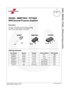
3 Onsemi is an Equal Opportunity/Affirmative Action Employer. This literature is subject to all applicable copyright laws and is not for resale in any manner. Other names and brands may be claimed as the property of others. Semiconductor Components Industries, LLC, 2005 November, 2005 Rev. 81 Publication Order Number:UC3842A/DUC3842A, UC3843A,UC2842A, UC2843 AHigh PerformanceCurrent Mode ControllersThe UC3842A, UC3843A series of high performance fixedfrequency current mode controllers are specifically designed foroff line and DC to DC converter applications offering the designer acost effective solution with minimal external components. Theseintegrated circuits feature a trimmed oscillator for precise duty cyclecontrol, a temperature compensated reference, high gain erroramplifier, current sensing comparator, and a high current totem poleoutput ideally suited for driving a power included are protective features consisting of input andreference undervoltage lockouts each with hysteresis, cycle by cyclecurrent limiting, programmable output deadtime, and a latch for singlepulse devices are available in an 8 pin dual in line plastic packageas well as the 14 pin plastic surface mount (SOIC 14).
4 The SOIC 14package has separate power and ground pins for the totem pole UCX842A has UYLO thresholds of 16 V (on) and 10 V (off),ideally suited for off line converters. The UCX843A is tailored forlower voltage applications having UVLO thresholds of V (on) V (off).Features Trimmed Oscillator Discharge Current for Precise Duty CycleControl Current Mode Operation to 500 kHz Automatic Feed Forward Compensation Latching PWM for Cycle By Cycle Current Limiting Internally Trimmed Reference with Undervoltage Lockout High Current Totem Pole Output Undervoltage Lockout with Hysteresis Low Startup and Operating Current Direct Interface with ON Semiconductor SENSEFET Products Pb Free Packages are Available14 SOIC 14D SUFFIXCASE 751A1 See detailed ordering and shipping information in the packagedimensions section on page 15 of this data INFORMATIONSee general marking information in the device markingsection on page 16 of this data MARKING INFORMATION18 PDIP 8N SUFFIXCASE 626 PIN CONNECTIONS(Top View)Vref(Top View)
5 CompensationVoltage FeedbackCurrent SenseRT/CTVrefVCCO utputGND12345678 CompensationNCVoltage FeedbackNCCurrent SenseNCRT/CTNCVCCVCO utputGNDP ower Ground123456798101112131418 SOIC 8D1 SUFFIXCASE 751 , UC3843A, UC2842A, UC2843 1. Simplified Block (12)VC7(11)Output6(10)PowerGround5(8)3(5 )CurrentSenseInputVref8(14)4(7)2(3)1(1)G ND5(9)RTCTV oltageFeedbackInputRR+ VrefUndervoltageLockoutOutputCompensatio nPin numbers in parenthesis are for the D suffix SOIC 14 RATINGSR atingSymbolValueUnitBias and Driver Voltages (Zero Series Impedance, see also Total Device spec)VCC, VC30 VTotal Power Supply and Zener Current(ICC + IZ)30mAOutput Current, Source or Sink (Note 1) Energy (Capacitive Load per Cycle) JCurrent Sense and Voltage Feedback InputsVin to + Amp Output Sink CurrentIO10mAPower Dissipation and Thermal CharacteristicsD Suffix, Plastic PackageMaximum Power Dissipation @ TA = 25 CThermal Resistance, Junction to AirN Suffix, Plastic PackageMaximum Power Dissipation @ TA = 25 CThermal Resistance, Junction to AirPDR JAPDR C/WW C/WOperating Junction TemperatureTJ+ 150 COperating Ambient TemperatureUC3842A, UC3843 AUC2842A, UC2843 ATA0 to + 70 25 to + 85 CStorage Temperature RangeTstg 65 to + 150 CMaximum ratings are those values beyond which device damage can occur.
6 Maximum ratings applied to the device are individual stress limitvalues (not normal operating conditions) and are not valid simultaneously. If these limits are exceeded, device functional operation is not implied,damage may occur and reliability may be Maximum Package power dissipation limits must be , UC3843A, UC2842A, UC2843 CHARACTERISTICS (VCC = 15 V, [Note 2], RT = 10 k, CT = nF, TA = Tlow to Thigh [Note 3],unless otherwise noted.)CharacteristicsSymbolUC284 XAUC384 XAUnitMinTypMaxMinTypMaxREFERENCE SECTIONR eference Output Voltage (IO = mA, TJ = 25 C) Regulation (VCC = 12 V to 25 V)Regline Regulation (IO = mA to 20 mA)Regload StabilityTS mV/ CTotal Output Variation over Line, Load, Noise Voltage (f = 10 Hz to 10 kHz,TJ = 25 C)Vn 50 50 VLong Term Stability (TA = 125 C for 1000 Hours)S mVOutput Short Circuit CurrentISC 30 85 180 30 85 180mAOSCILLATOR SECTIONF requencyTJ = 25 CTA = Tlow to Thighfosc474652 5760474652 5760kHzFrequency Change with Voltage (VCC = 12 V to 25 V) fosc/ V Change with TemperatureTA = Tlow to Thigh fosc/ T %Oscillator Voltage Swing (Peak to Peak)Vosc VDischarge Current (Vosc = V)TJ = 25 CTA = Tlow to AMPLIFIER SECTIONV oltage Feedback Input (VO = V) Bias Current (VFB = V)IIB AOpen Loop Voltage Gain (VO = V to V)AVOL6590 6590 dBUnity Gain Bandwidth (TJ = 25 C)
7 MHzPower Supply Rejection Ratio (VCC = 12 V to 25 V)PSRR6070 6070 dBOutput CurrentSink (VO = V, VFB = V)Source (VO = V, VFB = V) mAOutput Voltage SwingHigh State (RL = 15 k to ground, VFB = V)Low State (RL = 15 k to Vref, VFB = V) Adjust VCC above the Startup threshold before setting to 15 Low duty cycle pulse techniques are used during test to maintain junction temperature as close to ambient as C for UC3842A, UC3843 AThigh= +70 C for UC3842A, UC3843A 25 C for UC2842A, UC2843A+85 C for UC2842A, UC2843 AUC3842A, UC3843A, UC2842A, UC2843 CHARACTERISTICS (VCC = 15 V, [Note 4], RT = 10 k, CT = nF, TA = Tlow to Thigh [Note 5],unless otherwise noted.)UC284 XAUC384 XACharacteristicsSymbolMinTypMaxMinTypMa xUnitCURRENT SENSE SECTIONC urrent Sense Input Voltage Gain (Notes 6 & 7) Current Sense Input Threshold (Note 6) Supply Rejection RatioVCC = 12 to 25 V (Note 6)PSRR 70 70 dBInput Bias CurrentIIB 10 10 APropagation Delay (Current Sense Input to Output)tPLH(in/out) 150300 150300nsOUTPUT SECTIONO utput VoltageLow State (ISink = 20 mA)Low State(ISink = 200 mA)High State (ISink = 20 mA)High State(ISink = 200 mA)VOLVOH VOutput Voltage with UVLO ActivatedVCC = V, ISink = mAVOL(UVLO) Voltage Rise Time (CL = nF, TJ = 25 C)tr 50150 50150nsOutput Voltage Fall Time (CL = nF, TJ = 25 C)tf 50150 50150nsUNDERVOLTAGE LOCKOUT SECTIONS tartup Operating Voltage After Turn OnUCX842 AUCX843 AVCC(min) SECTIONDuty CycleMaximumMinimumDCmaxDCmin94 96 094 96 0%TOTAL DEVICEP ower Supply Current (Note 4)Startup.
8 (VCC = V for UCX843A,(VCC = 14 V for UCX842A) OperatingICC Supply Zener Voltage (ICC = 25 mA)VZ3036 3036 V4. Adjust VCC above the Startup threshold before setting to 15 Low duty cycle pulse techniques are used during test to maintain junction temperature as close to ambient as C for UC3842A, UC3843 AThigh= +70 C for UC3842A, UC3843A 25 C for UC2842A, UC2843A+85 C for UC2842A, UC2843A6. This parameter is measured at the latch trip point with VFB = 0 Comparator gain is defined as: AV V Output Compensation V Current Sense InputUC3842A, UC3843A, UC2842A, UC2843 , TIMING RESISTOR (k )Figure 2. Timing Resistor versusOscillator FrequencyFigure 3. Output Deadtime versusOscillator FrequencyFigure 4. Oscillator Discharge Currentversus TemperatureFigure 5. Maximum Output Duty Cycleversus Timing ResistorFigure 6. Error Amp Small SignalTransient ResponseFigure 7. Error Amp Large SignalTransient s/DIV20 mV/DIVVCC = 15 VAV = = 25 C10 k20 k50 k100 k200 k500 MfOSC, OSCILLATOR FREQUENCY (Hz)VCC = 15 VTA = 25 C10 k20 k50 k100 k200 k500 MfOSC, OSCILLATOR FREQUENCY (Hz)% DT, PERCENT OUTPUT DEADTIMEVCC = 15 VTA = 25 C 55 250255075100125TA, AMBIENT TEMPERATURE ( C), DISCHARGE CURRENT (mA)dischgIVCC = 15 VVOSC = VRT, TIMING RESISTOR ( ) k, MAXIMUM OUTPUT DUTY CYCLE (%)maxDVCC = 15 VCT = nFTA = 25 CIdischg = mAIdischg = VVCC = 15 VAV = = 25 s/DIV200 , UC3843A, UC2842A, UC2843 8.)
9 Error Amp Open Loop Gain andPhase versus FrequencyFigure 9. Current Sense Input Thresholdversus Error Amp Output VoltageFigure 10. Reference Voltage Changeversus Source CurrentFigure 11. Reference Short Circuit Currentversus TemperatureFigure 12. Reference Load RegulationFigure 13. Reference Line Regulation , OUTPUT VOLTAGE CHANGE ( mV/DIV) ms/DIVV , OUTPUT VOLTAGE CHANGE ( mV/DIV) ms/DIVVVCC = 12 V to 25 VTA = 25 C , REFERENCE VOLTAGE CHANGE (mV)ref020406080100120 Iref, REFERENCE SOURCE CURRENT (mA)VVCC = 15 VTA = 55 CTA = 125 C, REFERENCE SHORT CIRCUIT CURRENT (mA)SC 55 250255075100125TA, AMBIENT TEMPERATURE ( C)VCC = 15 VRL IVCC = 15 VIO = mA to 20 mATA = 25 C0 12 16 20 24110907050TA = 25 C 20 AVOL, OPEN LOOP VOLTAGE GAIN (dB)10 M10f, FREQUENCY (Hz)GainPhaseVCC = 15 VVO = V to VRL = 100 KTA = 25 k10 k100 M020406080100, EXCESS PHASE (DEGREES) 0VO, ERROR AMP OUTPUT VOLTAGE (V)0, CURRENT SENSE INPUT THRESHOLD ( = 15 VTA = 25 CTA = 55 CTA = 125 CUC3842A, UC3843A, UC2842A, UC2843 14.)
10 Output Saturation Voltageversus Load CurrentFigure 15. Output WaveformFigure 16. Output Cross ConductionFigure 17. Supply Current versusSupply Voltage50 ns/DIVVCC = 15 VCL = nFTA = 25 C100 ns/DIVVCC = 30 VCL = 15 pFTA = 25 C, SUPPLY CURRENT100 mA/DIV20 V/DIVI, OUTPUT VOLTAGEVCCO8006004002000IO, OUTPUT LOAD CURRENT (mA), OUTPUT SATURATION VOLTAGE (V)satVVCCTA = 25 CTA = 55 CGNDTA = 25 CSource Saturation(Load to Ground)TA = 55 CVCC = 15 V80 s Pulsed Load120 Hz Rate0 10203040, SUPPLY CURRENT (mA)CCVCC , SUPPLY VOLTAGEIRT = 10 kCT = nFVFB = 0 V ISense = 0 VTA = 25 CUCX843 AUCX842A90%10% Saturation(Load to VCC)UC3842A, UC3843A, UC2842A, UC2843 + Sink OnlyPositive True Logic=RS+InternalBiasReferenceRegulatorO scillatorSRQ (12)Q1 VinVCCVC7(11)6(10)5(8)3(5)+ (1)2(3)4(7)8(14)5(9)GNDO utputCompensationVoltage FeedbackInputRTCTVref PWML atchCurrent SenseComparatorRRPower GroundCurrent Sense numbers in parenthesis are for the D suffix SOIC 14 + ++ + + 18.