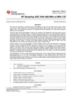
Transcription of Understanding High Speed ADC Testing and …
1 AN-835. APPLICATION NOTE. One Technology Way Box 9106 Norwood, MA 02062-9106, Tel: Fax: Understanding high Speed ADC Testing and Evaluation by Alex Arrants, Brad Brannon and Rob Reeder SCOPE DYNAMIC TEST HARDWARE SETUP. This document describes both the characterization and production SNR, SINAD, worst spur, and IMD are tested using a hardware test methods used by the high Speed Converter Group of Analog setup similar to that shown in Figure 1. In production tests, the Devices, Inc., to evaluate high Speed analog-to-digital converters test hardware is highly integrated, but the hardware principles (ADCs). While this application note should be considered a are the same. The basic setup for dynamic Testing includes a reference, it is not a substitute for a product data sheet. signal generator, band-pass filter, test fixture, low noise power supplies, encode source (often integrated on the evaluation board), data acquisition module, and data analysis software.
2 Analog Devices provides application hardware and software to aid in bench evaluation. WALL OUTLET. 100V TO 240V AC. 47Hz TO 63Hz SWITCHING. POWER. SUPPLY. SWITCHING. POWER. 6V DC. SUPPLY. 2A MAX. SIGNAL. SYNTHESIZER. 6V DC. 2A MAX. 4LO INPUT. ANALOG INPUT. SIGNAL. SYNTHESIZER. AGILENT PC. POWER SUPPLY RUNNING ADC. ANALYZER. OR VISUAL ANALOG. OPTIONAL CW I/Q USER SOFTWARE. CLOCK OUTPUTS SPECTRUM. INPUT ANALYZER OSCILLOSCOPE. GAIN CONTROL OR. INPUT SIGNAL. 05941-001. SYNTHESIZER. Figure 1. Typical Characterization Test Setup Rev. B | Page 1 of 28. AN-835 Application Note TABLE OF CONTENTS. Scope .. 1 Common-Mode Rejection Ratio (CMRR, dB) .. 19. Dynamic Test Hardware Setup .. 1 Aperture Delay (AD, ps).. 20. Revision History .. 3 Aperture Jitter or Aperture Uncertainty (ps RMS) .. 21. HSC-ADC-EVALC Evaluation Platform.
3 4 Crosstalk (dB) .. 21. Background .. 5 Input-Referred Noise (LSB RMS) .. 21. Analog Signal Source .. 6 Out-of-Range Recovery Time (CLK Cycles) .. 21. Analog Signal Filter .. 6 Digital Time Domain .. 21. Encode Signal Sources .. 7 Conversion Error Rate (CER).. 24. Power Supplies .. 8 DC Test Definitions .. 25. Data Acquisition .. 8 Gain Error (%FS).. 25. AC Test Definitions .. 9 Gain Matching (%FS) .. 25. FFT 9 Offset Error (%FS) .. 25. Single-Tone FFT .. 9 Offset Matching (mV) .. 25. Two-Tone FFT .. 12 Temperature Drift (ppm) .. 25. Noise Power Ratio (NPR, dB) .. 14 Voltage Output high /Voltage Output Low (VOH/VOL, V) .. 25. Full Power Bandwidth (MHz) .. 15 25. Dither Testing .. 16 Power Supply Rejection Ratio (PSRR, dB) .. 27. Analog Input .. 17 References .. 28. Analog Input Full-Scale Range (V p-p) .. 18 Additional References.
4 28. Common-Mode Input Range (V) .. 19. Rev. B | Page 2 of 28. Application Note AN-835. REVISION HISTORY. 3/15 Rev. A to Rev. B Changes to Figure 13 .. 11. Deleted ADIsimADC 5 Changes to Figure 14 .. 13. Changes to Figure 24 ..20 Changes to Figure 17 .. 14. Changes to Gain Matching (%FS) Section ..25 Changes to Figure 19 .. 15. Changes to Dither Testing and Figure 20 .. 16. 6/10 Rev. 0 to Rev. A Changes to Figure 21 .. 17. Added Alex Arrants to by .. 1 Changes to Figure 22 .. 18. Changes to Dynamic Test Hardware Setup Section and Changes to Common-Mode Input Range (V) Section, Common- Figure 1 .. 1 Mode Rejection Ratio (CMRR, dB) Section, and Figure 23 .. 19. Changes to HSC-ADC-EVALC Evaluation Platform Section Changes to Aperture Delay (AD, ps) Section and Figure 24 .. 20. and Figure 4 Changes to Input-Referred Noise (LSB RMS) 21.
5 Changes to Figure 3, ADIsimADC Section, and Figure 4 .. 5 Added Figure 26 .. 21. Changes to Analog Signal Source Section, Analog Signal Filter Changes to Pipeline Delay (CLK Cycles) Section .. 22. Section, Figure 5, and Figure 6 .. 6 Added Figure 27 .. 22. Changes to Encode Signal Sources Section .. 7 Changes to Figure 28 .. 23. Changes to Figure 10, Power Supplies Section, Figure 11, and Changes to Conversion Error Rate (CES) Section and Data Acquisition Section .. 8 Table 1 .. 24. Added Figure 12; Renumbered Sequentially .. 8 Added Figure 29 .. 24. Changes to User-Defined Signal-to-Noise Ratio (UDSNR, dB) Changes to References Section .. 28. Section and Noise Figure (NF, dB) Section .. 9. Changes to Noise Floor (dBFS) Section and Effective Number 4/06 Revision 0: Initial Version of Bits (ENOB, Bits) Section.
6 10. Rev. B | Page 3 of 28. AN-835 Application Note HSC-ADC-EVALC EVALUATION PLATFORM The FPGA-based buffer memory board can be connected to a The high Speed ADC FIFO evaluation kit (HSC_ADC_EVALC) PC through a standard USB cable and used with the VisualAnalog includes a FPGA-based buffer memory board to capture blocks and SPIC ontroller software to quickly evaluate the performance of digital data from Analog Devices high Speed ADC evaluation of the high Speed ADCs. Users can change settings in the SPI. boards, VisualAnalog , and SPIC ontroller software. For more registers unique to the individual ADC product, view an FFT. information on the HSC-ADC-EVALC evaluation platform, visit for a specific analog input and sample rate, and analyze SNR, SINAD, SFDR, and harmonic information, as well as time domain information, such as gain and offset.
7 The HSC-ADC-EVALC. supports CMOS, LVDS, and CML outputs. Some boards may require an interposer or slightly different FIFO alternative. If additional or different hardware is necessary, it will be specified in the product data sheet. For more detailed information on the HSC-ADC-EVALC, the SPIC ontroller, and how the VisualAnalog software works, visit POWER ON-BOARD HSC-ADC-EVALC. VOLTAGE USB. CONNECTOR. REGULATORS. SINGLE OR MULTICHANNEL FPGA. high Speed ADC CONFIGURATION LED2 LED1 UPLOAD CAPTURE. EVALUATION BOARD MODE. PORTB. DATA BUS 2(18) DATA(16) PORTD. FILTERED n J3* J6. ANALOG CLKA(2) FIFO. CONTROL(9) USB. LOGIC. INPUT FPGA CONTROLLER. ADC USB. DATA BUS 1(18) PORTC CONNECTOR. n J2* PORTE. CLKB(2). PORTA STANDARD. EXT SYNC1 USB CLOCK FPGA. DONE USB. CIRCUIT CONFIG ONBOARD. EXT SYNC2 VOLTAGE J4. PROM. REGULATORS.
8 FPGA. CONFIG POWER. PROM CONNECTOR. FPGA GPIO(8). J1* SPI(7) RECONFIG. SPI. USB DIRECT(5). J10. *DATA CONVERTER I/O CONNECTORS JTAG. 05941-002. CONNECTOR. CLOCK INPUT. Figure 2. Typical HSC-ADC-EVALC Evaluation Platform Rev. B | Page 4 of 28. Application Note AN-835. BACKGROUND. GENERAL PURPOSE I/O, USB/SPI CONTROL DATA BUS 1 DATA BUS 2. FPGA LOAD. SELECT. XILINX. VIRTEX-4. FPGA. DEBUG ON BOARD. PINS POWER SUPPLY. 100 MHz OSCILLATOR. EXTERNAL. SYNC I/O. FPGA I/O. VOLTAGE MODE. FPGA CONFIG. PROM. 05941-003. CYPRESS USB USB CONNECTOR FPGA JTAG 5 VDC POWER. CONTROLLER CONNECTOR INPUT. Figure 3. HSC-ADC-EVALC: FPGA-Based Data Capture Board 05941-004. Figure 4. VisualAnalog: Typical Canvas Showing an FFT and Time Domain Performance Plots Rev. B | Page 5 of 28. AN-835 Application Note 0. ANALOG SIGNAL SOURCE IL @ 10 MHz Usually, dynamic Testing employs a Rohde & Schwarz SMA/ 10.
9 SMHU/SMG/SMGU, an Agilent 8644 signal generator, a Wenzel crystal oscillators or a Valpey Fisher crystal oscillator. These ATTENUATION (dB). 20. sources have proven to provide exceptional performance (low phase noise, flat frequency response, and reasonable harmonic 30. performance) for frequencies of a few kilohertz to those of a few gigahertz. Harmonic performance of these generators is typically 40. not as good as the intrinsic linearity of a given ADC, mandating the need for additional filtering between the signal generator 50. and the analog input to the ADC. 60. 05941-005. ANALOG SIGNAL FILTER 40 60 80 100 120. FREQUENCY (MHz). Both fixed frequency and tunable frequency band-pass filters Figure 5. Typical Performance of TTE's J97. are used for device Testing . The fixed frequency filters are typically 0. smaller than tunable filters and often provide slightly better performance.
10 Tunable filters allow Testing across a wide range 10. of frequencies using one filter. Several filter manufacturers, including IL 3dB @ 100 MHz K&L Microwave, TTE, and Allen Avionics, Inc., provide excellent ATTENUATION (dB). 20. filters for ADC Testing . There are two types of filters that are often used for ADC Testing : 30. low-pass filters and band-pass filters. These can be used individually or combined to yield the level of performance 40. required for an application. 50. Low-pass filters are a good choice when a wide range of analog frequencies must be applied to the ADC. However, they allow 60. 08941-006. 85 90 95 100 105 110 115. noise to pass from the signal generator to the ADC. This noise FREQUENCY (MHz). may reduce the level of performance measured for the ADC. A. Figure 6. Typical Band-Pass Performance of TTE's Q70T.