Lecture 12: MOS Transistor Models
Current in transistor is very low until the gate voltage crosses the threshold voltage of device (same threshold voltage as MOS capacitor) Current increases rapidly at first and then it finally reaches a point where it simply increases linearly VGS IDS VT VGS IDS VDS
Download Lecture 12: MOS Transistor Models

Information
Domain:
Source:
Link to this page:
Documents from same domain
Diodes and Transistors
inst.eecs.berkeley.eduDiodes and Transistors 1. ... basic semiconductor physics. We won’t discuss the details because the point of this ... switch. Below the specified ...
HSPICE Tutorial - University of California, Berkeley
inst.eecs.berkeley.eduHSPICE Tutorial Contents 1 Introduction 1 ... ee105 spice tutorial example 1 - simple rc circuit in the Results Browser and double-clicking vs and vo to plot them in the graph. You may have been able to guess from the netlist, but you’ll see that vsis a …
Introduction to LabVIEW - University of California, …
inst.eecs.berkeley.eduIntroduction to LabVIEW 1. Introduction Welcome to the LabVIEW component of EE100! This lab is just a simple introduction to the graphical circuit simulation ...
Introduction to LabVIEW For Use in Embedded …
inst.eecs.berkeley.eduUC Berkeley EE249 Hugo.Andrade@ni.com Introduction to LabVIEW For Use in Embedded System Development
EE105 –Fall 2015 Microelectronic Devices and Circuits
inst.eecs.berkeley.eduSummary of MOS Single-Transistor Amplifiers MOS Common Source Common Source with Deg. Common Drain Common Gate Ri ∞ ∞ ∞ Small Ro Large Very Large Small Large
Introduction to Digital Systems - University of …
inst.eecs.berkeley.eduDepartment of EECS EE100/42-43 Spring 2007 Rev. 1 Introduction to Digital Systems 0. Acknowledgments Many thanks to Prof. Bernhard Boser and National Instruments for funding this project in the
EE126: Probability and Random Processes - Lecture 1 ...
inst.eecs.berkeley.eduprobability 4 The probabilities summed over all of the base outcomes always equals 1 Example: Toss a fair coin twice 1 Base outcomes are HH,HT,TH,TT 2 This covers all the possibilities. M.E. 3 Each of these outcomes is equally likely 4 Assign each outcome a probability of 0:25. The list (set) of base outcomes is called the Sample Space.
EECS 126 Probability and Random Processes: Course Syllabus ...
inst.eecs.berkeley.eduDescription: Probability is a mathematical discipline that allows one to reason about uncertainty: it helps us to predict uncertain events, to make better decisions under uncertainty, and to design and build systems. Throughout the course, we will teach you the fundamental ideas of probability and random processes along with the labs.
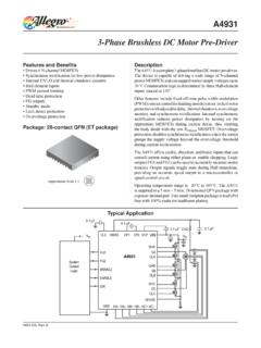
3-Phase Brushless DC Motor Pre-Driver
inst.eecs.berkeley.eduDescription The A4931 is a complete 3-phase brushless DC motor pre-driver . The device is capable of driving a wide range of N-channel power MOSFETs and can support motor supply voltages up to
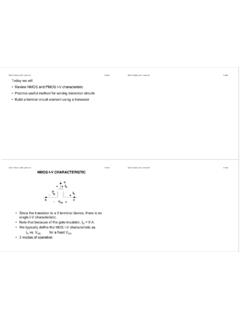
DS -V I G - EECS Instructional Support Group Home Page
inst.eecs.berkeley.eduG D S I D I G-V DS + + V G S _ NMOS I-V CHARACTERISTIC • Since the transistor is a 3-terminal device, there is no single I-V characteristic. • Note that because of the gate insulator, I G = 0 A. • We typically define the MOS I-V characteristic as I D vs. V DS for a fixed V GS. • 3 modes of operation
Related documents

Lecture11-MOS Cap Delay
bwrcs.eecs.berkeley.eduMOS Transistor as a Switch Saw that real transistors aren’t exactly resistors Look more like current sources in saturation Two questions: Which region of IV curve determines delay? How can that match up with the RC model? EE141 29 EECS141 Lecture #11 29 Transistor Driving a Capacitor • With a step input: ID VDS VDD /2 VDD VDD ÆVDD/2 VGS ...
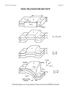
MOS TRANSISTOR REVIEW - Stanford University
web.stanford.eduMOS Transistor 5 In reality constant field scaling has not been observed strictly. Since the transistor current is proportional to the gate overdrive (VG-VT), high performance demands have dictated the use of higher supply voltage. However, higher supply voltage implies increased power dissipation (CV2f). In the recent past low power ...

Lecture 15: MOS Transistor models: Body effects, SPICE models
inst.eecs.berkeley.edutransistor (BJT): Chapter 7 zThen go on to design of transistor amplifiers: chapter 8 Department of EECS University of California, Berkeley EECS 105 Spring 2004, Lecture 15 Prof. J. S. Smith MOS operation zAn inversion mode MOS transistor operates by producing a sheet carriers just under the oxide zThe names source and drain are picked so that the
Lecture 24 MOSFET Basics (Understanding with no math ...
alan.ece.gatech.eduMOS Transistor Qualitative Description Assume an n-channel (receives it’s name from the “type” of channel present when current is flowing) device with its source and substrate grounded (i. e., V S =V B =0 V). For any value of V DS: •when V GS <0 (accumulation), the source to drain path consists of two back to back diodes.

8. MOS Transistors, CMOS Logic Circuits
web.stanford.eduMOSFET a.k.a. MOS Transistor • Are very interesting devices –Come in two “flavors” –pMOSand nMOS –Symbols and equivalent circuits shown below • Gate terminal takes no current (at least no DC current) –The gate voltage*controls whether the “switch” is ON or OFF pMOS nMOS R on gate * actually, the gate –to –source voltage ...

MOS Transistor Theory
people.ee.duke.eduMOS Transistor Theory • Study conducting channel between source and drain • Modulated by voltage applied to the gate (voltage-controlled device) • nMOS transistor: majority carriers are electrons (greater mobility), p-substrate doped (positively doped) • pMOS transistor: majority carriers are holes (less

5 MOS Field-Effect Transistors (MOSFETs)
learninglink.oup.com5 MOS Field-Effect Transistors (MOSFETs) Section 5.1: Device Structure and Physical Operation 5.1 An NMOS transistor is fabricated in a 0.13-µm CMOS process with L = 1.5Lmin and W = 1.3 µm. The process technology is specified to have tox =2.7nm, μn =400cm2/V·s, and Vtn =0.4V. (a) Find Cox, kn,andkn. (b) Find the overdrive voltage VOV and ...
MOS Capacitances - University of California, Berkeley
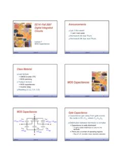
bwrcs.eecs.berkeley.eduMOS Capacitances EE141 2 ... –Way off, off, transistor linear, transistor saturated. EE141 7 EECS141 Lecture #7 7 Transistor In Cutoff When the transistor is off, no carriers in channel to form the other side of the capacitor. –Substrate acts as the other capacitor terminal

Bipolar Transistor
www.chu.berkeley.eduIt was the first mass produced transistor, ahead of the MOS field-effect transistor (MOSFET) by a decade. After the introduction of metal-oxide-semiconductor (MOS) ICs around 1968, the high-density and low-power advantages of the MOS technology steadily eroded the BJT’s early dominance. BJTs are still pref erred in some high-frequency and analog