Op-Amp/Comparator Application Note - Rohm
Each op-amp circuit is composed of five terminals: a power supply terminal on the positive side, a power supply terminal on the negative side, a + input terminal, a - input terminal, and an output terminal. (There are no general terms for the terminals except classifications such as power source, input and output.) Table 1.1.1.
Download Op-Amp/Comparator Application Note - Rohm

Information
Domain:
Source:
Link to this page:
Documents from same domain
SiC Power Devices and Modues Application Note
fscdn.rohm.com600V 400V 100V Si C D D D D G2GG 3ÿ G2GG H 9×3ÿ FÜ SiFÜ 8 æ GG ö G ì e Majority carrier device : High speed Minority carrier device : Low on-resistance, but low speed ・ Significant reduction in recovery loss ・ Downsizing of devices by increase in frequency Can be manufactured in this area, but little advantage over Si
Linear Regulator IC Series Linear Regulator 기초
fscdn.rohm.comLinear Regulator 는 기본적으로 입력, 출력, GND 핀으로 구성되며, 출력이 가변일 경우는 출력전압의 귀환이 필요 하기 때문에 귀환(Feedback)핀이 추가됩니다. (Figure 1) IN OUT FB GND V IN V O Figure 1. Linear Regulator 의 기본구성 Linear Regulator 내부회로의 개요는 Figure 2 …
Efficiency of Buck Converter
fscdn.rohm.comEfficiency of Buck Converter Switching regulators are known as being highly efficient power sources. To further improve their efficiency, it is helpful to understand the basic mechanism of power loss. This application note explains power loss factors and methods for calculating them.
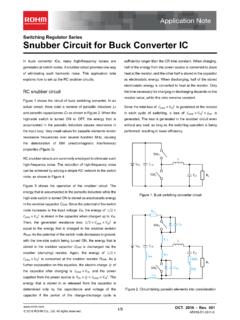
Snubber Circuit for Buck Converter IC : Power Management
fscdn.rohm.comSnubber Circuit for Buck Converter IC AEK59-D1-0311-0 For example, when the input voltage VIN is 24 V and the switching frequency fSW is 1 MHz, 2 Ë Ì Ç » L680 pF H24 6 H1 MHz L0.39 W the generated consumption power of 0.39 W requires a 6432 size resistor (2512 in inches) with a rated power of 1 W.
ISO 26262: Functional Safety Standard for Modern Road …
fscdn.rohm.comIntrinsic safety is a method for ensuring safety by removing the causes of danger. Functional safety, on the other hand, is a method of reducing risks to an acceptable level to ensure safety ... verification, prototyping, and evaluation are clarified, with reviews performed at each stage. It is also necessary to manage the documents created at
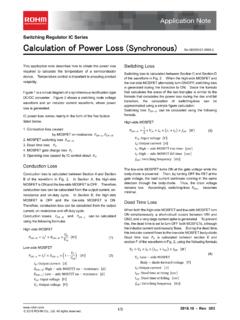
Calculation of Power Loss (Synchronous) : Power Management
fscdn.rohm.comCalculation of Power Loss (Synchronous) This application note describes how to obtain the power loss required to calculate the temperature of a semiconductor device. Temperature control is important to ensuring product reliability. Figure 1 is a circuit diagram of a synchronous rectification type DC/DC converter. Figure 2 shows a switching node ...
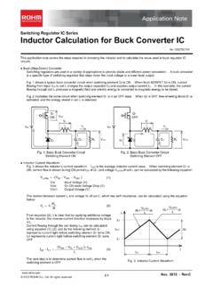
Inductor Calculation for Buck Converter IC
fscdn.rohm.comInductor Calculation of Buck Converter Current-difference between max. and min. (ILP-ILT) is as follows: IN SW D SW IN SW OUT D OUT LP LT V V V L f V V V V V I I (15) Equations (13) and (15) show that large inductance L and high switching frequency will reduce maximum current (ILP)and current difference between max. and min. (ILP-ILT).
Hysteresis Setting for Comparator - Rohm
fscdn.rohm.comprovided only to illustrate the standard usage and operations of the Products. The peripheral conditions must be taken into account when designing circuits for mass production. The technical information specified herein is intended only to show the typical functions of and examples of application circuits for the Products.
Snubber circuit design methods - Rohm
fscdn.rohm.comis bulk capacitor placed in parallel with input HVdc-PGND. During the turn off of LS, surge voltage occurs in drain-source of LS by resonant phenomenon between L MAIN and parasitic capacitance of the MOSFET C OSS ( C DS + DG). The maximum voltage V DS_SURGE is as shown in (1). Where V HVDC is the applied voltage on HVdc terminal and R OFF

ROHM Switching Regulator Solutions Synchronous Buck ...
fscdn.rohm.comROHM Switching Regulator Solutions Synchronous Buck Converter Controller BD9611MUV-EVK-001 Description Using a synchronous rectified step-down DC/DC converter IC BD9611MUV BD 9611MUV-EVK-001 evaluation board 15.0 V ~ output a 24 V input voltage 12.0 V. Provides 10.0A output current. Output current is possible with current settings by selecting
Related documents
MT-043: Op Amp Power Supply Rejection Ratio (PSRR) and ...
www.analog.comPOWER SUPPLY REJECTION RATIO (PSRR) If the supply of an op amp changes, its output should not, but it typically does. If a change of X volts in the supply produces an output voltage change of Y volts, then the PSRR on that supply (referred to the output, RTO) is X/Y. The dimensionless ratio is generally called the power supply rejection ratio ...

Understanding power supply ripple rejection in linear ...
www.ti.comUnderstanding power supply ripple rejection in linear regulators Power supply ripple rejection ratio (PSRR) is a measure of how well a circuit rejects ripple coming from the input power supply at various frequencies and is very critical in many RF and wireless applications. In the case of an LDO, it is a measure of the output ripple compared to ...
MCP6001/1R/1U/2/4 - 1 MHz, Low-Power Op Amp
ww1.microchip.comMay 14, 2019 · Power Supply Rejection Ratio PSRR — 86 — dB V CM = VSS Input Bias Current and Impedance Input Bias Current: IB — ±1.0 — pA Industrial Temperature IB —19 — pATA = +85°C Extended Temperature IB — 1100 — pA TA = +125°C Input Offset Current I OS — ±1.0 — pA Common-Mode Input Impedance Z CM —10 13||6 — ||pF
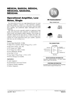
NE5534 - Operational Amplifier, Low Noise, Single
www.onsemi.comCommon Mode Rejection Ratio CMRR 70 100 − 80 100 − dB Power Supply Rejection Ratio PSRR − 10 100 − 10 50 V/V Large-Signal Voltage Gain A VOL R L ≥ 600 ,
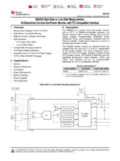
INA226 High-Side or Low-Side Measurement, Bi-Directional ...
www.ti.com• 16 Programmable Addresses of the supply voltage. The device operates from a • Operates from 2.7-V to 5.5-V Power Supply single 2.7-V to 5.5-V supply, drawing a typical of 330 • 10-Pin, DGS (VSSOP) Package μA of supply current. The device is specified over the operating temperature range between –40°C and

FEATURES DESCRIPTIO U - Analog Devices
www.analog.comCMRR Common Mode Rejection Ratio VCM = 0.1V to 3.2V 90 103 87 102 dB PSRR Power Supply Rejection Ratio VS = ±2V to ±18V, VO = 0V 100 117 97 116 dB Maximum Output Voltage Swing Output Low, 600Ω to GND 615 6 18 mV Output High, 600Ω to GND 3.2 3.8 3.1 3.8 V IS Supply Current 380 630 400 680 µA

1A LOW DROPOUT ADJUSTABLE AND FIXED ... - Diodes …
www.diodes.comPSRR Power Supply Rejection Ratio (Note 8) f = 1KHz, I OUT = 100mA 60 65 dB f = 10KHz, I OUT = 100mA 45 t ST Start-Up Time V OUT = 3V, C OUT 200= 1µF, R L = 30Ω µs û7 A VOUT û9287 Output Voltage Temperature Coefficient I OUT = 100mA, -40 °C≤ T A ≤ +85 ±130 ppm/°C T SHDN Thermal Shutdown Threshold 150 °C T