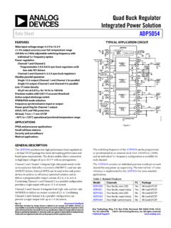
Quad Buck Regulator Integrated Power Solution Data Sheet ...
discharge switch + – q3 q4 uvlo3 pvin3 sw3 bst3 vreg vreg driver driver pgnd3 control logic and mosfet driver with anticross protection en3 0.8v 1mΩ hiccup and latch-up ocp comp3 0.8v clk3 slope comp clk3 0.72v pwrgd3 zero cross + – + – freq foldback + – + – channel 3—buck duplicate channel 3 channel 4—buck current balance en4 ...
Download Quad Buck Regulator Integrated Power Solution Data Sheet ...

Information
Domain:
Source:
Link to this page:
Documents from same domain

AD743 Ultralow Noise BiFET Op Amp Data Sheet …
www.analog.comREV. E Information furnished by Analog Devices is believed to be accurate and reliable. However, no responsibility is assumed by Analog Devices for its

MT-070: In-Amp Input RFI Protection - Analog …
www.analog.comRev.0, 10/08, WK Page 1 of 6 MT-070 TUTORIAL In-Amp Input RFI Protection . PROTECTING IN-AMPS AGAINST RFI . Real-world applications must deal with an ever increasing amount of radio frequency

LTC3108 - Ultralow Voltage Step-Up Converter and …
www.analog.comLTC3108 3108fc For more information www.linear.com/LTC3108 LDO

1.8 V Low Power CMOS Rail-to-Rail Input/Output …
www.analog.com1.8 V Low Power CMOS Rail-to-Rail Input/Output Operational Amplifier Data Sheet AD8515 Rev. E Document Feedback Information furnished by Analog Devices is believed to be accurate and reliable.

Low Cost Micropower, Low Noise CMOS Rail-to …
www.analog.comLow Cost Micropower, Low Noise CMOS Rail-to-Rail, Input/Output Operational Amplifiers Data Sheet AD8613/AD8617/AD8619 Rev. H Document Feedback Information furnished by Analog Devices is believed to be accurate and reliable.

Low Cost CMOS, High Speed, Rail-to-Rail Amplifiers
www.analog.comLow Cost CMOS, High Speed, Rail-to-Rail Amplifiers Data Sheet ADA4891-1/ADA4891-2/ADA4891-3/ADA4891-4 Rev. F Document Feedback Information furnished by Analog Devices ...

Zero-Drift, Single-Supply, Rail-to-Rail Input/Output ...
www.analog.comZero-Drift, Single-Supply, Rail-to-Rail Input/Output Operational Amplifier Data Sheet AD8628/AD8629/AD8630 FEATURES Lowest auto-zero amplifier noise Low offset voltage: 1 µV AD8628

FEATURES DESCRIPTIO U - analog.com
www.analog.com1 LT1025 1025fb DESCRIPTIO U APPLICATIO S U 80µA Supply Current 4V to 36V Operation 0.5°C Initial Accuracy (A Version) Compatible with Standard Thermocouples (E, J, K, R, S, T) Auxiliary 10mV/°C Output Available in 8-Lead PDIP and SO Packages Thermocouple Cold Junction Compensator Centigrade Thermometer Temperature …

LT1173 - Micropower DC/DC Converter Adjustable …
www.analog.comLT1173 1 Micropower DC/DC Converter Adjustable and Fixed 5V, 12V VOUT 5V/DIV 0V PROGRAM 5V/DIV 5ms/DIV 1173 TA02 L1* 100µH LT1173 • TA01 + GND SW2 FB SW1 ILIM VIN 10 F LT1173

AD9850 CMOS, 125 MHz Complete DDS …
www.analog.comrev. h a cmos, 125 mhz complete dds synthesizer ad9850 functional block diagram clock out clock out analog in analog out dac rset …
Related documents

Switch Mode Power Supply (SMPS) Topologies
ww1.microchip.comSep 10, 2007 · Buck Converter A buck converter, as its name implies, can only produce lower average output voltage than the input voltage. The basic schematic with the switching waveforms of a buck converter is shown in Figure 2. In a buck converter, a switch (Q1) is placed in series with the input voltage source V IN. The input source VIN
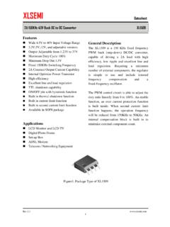
XL1509 Datasheet - xlsemi.com
www.xlsemi.com2A 150KHz 40V Buck DC to DC Converter XL1509 Rev 2.3 www.xlsemi.com ... 3.3V R 2=4 .2K 12V R2=21 .8K Switch 3 Figure3. Function Block Diagram of XL1509 Typical Application Circuit XL1 509-5.0 CIN O C1 1 05 1 80uf 35V D1 L1 68uh/2A +1 2V LOAD 1 5~8 4 2 GND VIN

Datasheet - XLSEMI芯龙半导体 首页
xlsemi.com4 5 TO252-5L Metal Tab GND Figure2. Pin Configuration of XL7025 (Top View) Table 1 Pin Description Pin Number Pin Name Description 1 VIN Supply Voltage Input Pin. Bypass Vin to GND with a suitably large capacitor to eliminate noise on the input. 2 SW Power Switch Output Pin (SW). Output is the switch node that supplies power to the output. 3 GND
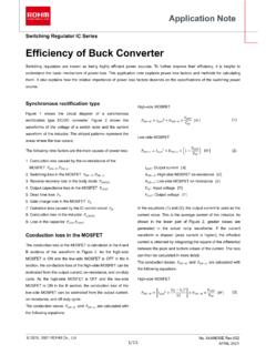
Efficiency of Buck Converter - Rohm
fscdn.rohm.comEfficiency of Buck Converter ... waveforms of the voltage of a switch node and the current waveform of the inductor. The striped patterns represent the areas where the loss occurs. The following nine factors are the main causes of power loss: 1. Conduction loss caused by the on-resistance of the ... 4. Output capacitance loss in the MOSFET ...
Switch Mode Power Supply (SMPS) Topologies
ww1.microchip.comSep 10, 2007 · Buck Converter A buck converter, as its name implies, can only produce lower average output voltage than the input voltage. The basic schematic with the switching waveforms of a buck converter is shown in Figure 2. In a buck converter, a switch (Q1) is placed in series with the input voltage source V IN. The input source VIN
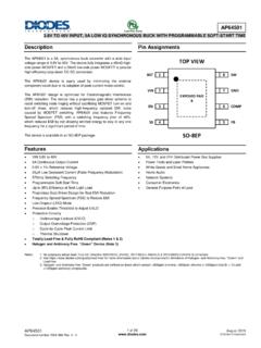
TOP VIEW - Diodes Incorporated
www.diodes.comSW Switch Pin Voltage-0.3 to VIN + 0.3 (DC) V-2.5 to VIN + 2.0 (20ns) T ST Storage Temperature -65 to +150 °C T J Junction Temperature +160 °C T L Lead Temperature +260 °C ESD Susceptibility (Note 5) HBM Human Body Model 2000 V …
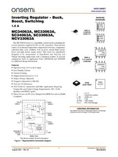
MC34063A - Inverting Regulator - Buck, Boost, Switching 1.5 A
www.onsemi.comInverting Regulator - Buck, Boost, Switching 1.5 A MC34063A, MC33063A, SC34063A, SC33063A, ... 5 4 6 7 Drive 8 Collector Ipk Sense VCC Comparator Inverting Input Switch Switch Emitter Timing Capacitor GND (Bottom View) ... Switch Emitter Voltage (VPin 1 = 40 V) VE(switch) 40 Vdc

Under the Hood of a DC/DC Boost Converter
www.ti.comUnlike a buck-derived topology, energy flows to the load during the OFF time of the control switch. The effect of any control action during the ON time of the switch is delayed until the switch is turned OFF. For example, during a load-step increase, the output voltage drops due to insufficient stored energy in the inductor. The
Switching regulator fundamentals (Rev. C)
www.ti.comON time of the switch. 2 Switching Converter Topologies The most commonly used DC/DC converter circuits will now be presented along with the basic principles of operation. 2.1 Buck Regulator The most commonly used switching converter is the Buck, which is used to down-convert a DC voltage to a lower DC voltage of the same polarity.