
Switch Mode Power Supply (SMPS) Topologies
Sep 10, 2007 · waveforms of a buck converter is shown in Figure 2. In a buck converter, a switch (Q1) is placed in series with the input voltage source V IN. The input source VIN feeds the output through the switch and a low-pass filter, implemented with an inductor and a capacitor. In a steady state of operation, when the switch is ON for
Download Switch Mode Power Supply (SMPS) Topologies
Information
Domain:
Source:
Link to this page:
Documents from same domain

Power Factor Correction in Power Conversion …
ww1.microchip.com© 2007 Microchip Technology Inc. DS01106A-page 2 AN1106 FIGURE 1: CURRENT WAVEFORMS WITH AND WITHOUT PFC These waveforms illustrate that …

2.7V to 5.5V Single Supply CMOS Op Amp
ww1.microchip.comMCP601/1R/2/3/4 DS21314G-page 2 © 2007 Microchip Technology Inc. 1.0 ELECTRICAL CHARACTERISTICS Absolute Maximum Ratings † VDD –VSS.....7.0V

Data Encryption Routines for PIC24 and dsPIC Device
ww1.microchip.com© 2006 Microchip Technology Inc. DS01044A-page 1 AN1044 INTRODUCTION Currently, there are three data encryption standards approved …

Using SAM-BA for Linux on SAMA5D3 Xplained
ww1.microchip.comAN-8995 – Using SAM-BA for Linux on SAMA5D3 Xplained: 42328A−06/2014 Page 5 of 19 2. Setup With Ubuntu distributions, a user has to be member of the dialout group to access serial devices like

MCP6021/1R/2/3/4 - Rail-to-Rail Input/Output, 10 …
ww1.microchip.com2001-2017 Microchip Technology Inc. DS20001685E-page 1 MCP6021/1R/2/3/4 Features • Rail-to-Rail Input/Output • Wide Bandwidth: 10 MHz (typical)

Low Quiescent Current LDO - Microchip Technology
ww1.microchip.com2005-2016 Microchip Technology Inc. DS20001826D-page 1 MCP1700 Features: • 1.6 µA Typical Quiescent Current • Input Operating Voltage Range: 2.3V to 6.0V

MCP1703 250 mA, 16V, Low Quiescent Current
ww1.microchip.com2010 Microchip Technology Inc. DS22049E-page 1 MCP1703 Features: • 2.0 µA Typical Quiescent Current • Input Operating Voltage Range: 2.7V to16.0V

MTCH6102 Low-Power Projected Capacitive Touch …
ww1.microchip.com2014 Microchip Technology Inc. DS40001750A-page 1 Description: Microchip’s MTCH6102 is a turnkey projected capacitive touch controller that simplifies adding

PIC32 GUI Development Board with Projected …
ww1.microchip.comPIC32 GUI Development Board with Projected Capacitance (PCAP) Touch Information Sheet Microchip Technology Inc.

RN4020 Bluetooth Low Energy Module User’s Guide
ww1.microchip.comRN4020 BLUETOOTH LOW ENERGY MODULE USER’S GUIDE 2014 Microchip Technology Inc. DS70005191B-page 7 Preface INTRODUCTION This chapter contains general information that will be useful to know before using the
Related documents
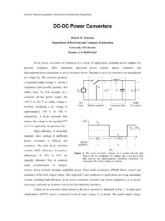
DC-DC Power Converters
ecee.colorado.educurrent, including high-efficiency dc-ac power converters (inverters and power amplifiers), ac-ac power converters, and some ac-dc power converters (low-harmonic rectifiers). A basic dc-dc converter circuit known as the buck converter is illustrated in Fig. 1. A single-pole double-throw (SPDT) switch is connected to the dc input voltage V g as ...
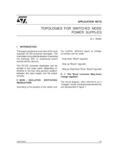
Topologies for switch mode power supplies
www.st.coma single non dissipative way to systematically clamp the voltage across the switches to the input DC voltage V in. This energy recovery system allows us to work at higher switching frequencies and with a better efficiency than that of the single switch structure. However, the double switch structure requires driving a high side switch.
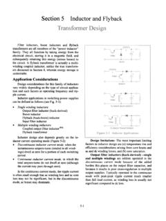
'Magnetics Design 5 - Inductor and Flyback Transformer …
www.ti.comfactors in inductor design are (a) temperature rise and efficiency considerations arising from core losses and ac and dc winding losses, and (b) core saturation. Output filter inductors (buck-derived) --single and multiple windings are seldom operated in the discontinuous current mode because of the added
Quad Buck Regulator Integrated Power Solution Data Sheet ...
www.analog.comProgrammable 2 A/4 A/6 A sync buck regulators with low-side FET drivers Channel 3 and Channel 4: 2.5 A sync buck regulators Flexible parallel operation Single 12 A output (Channel 1 and Channel 2 in parallel) Single 5 A output (Channel 3 and Channel 4 in parallel) Low 1/f noise density 40 μV rms at 0.8 V REF for 10 Hz to 100 kHz
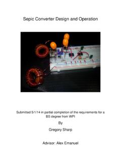
Sepic Converter Design and Operation
web.wpi.eduMay 01, 2014 · Buck-boost converters can be cheaper because they only require a single inductor and a capacitor. However, these converters suffer from a high amount of input current ripple. This ripple can create harmonics; in many applications these harmonics necessitate using a large capacitor or an LC filter. This often makes the buck-boost expensive or
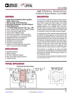
LTC3780 (Rev G) - Analog Devices
www.analog.comHigh Efficiency Buck-Boost Converter n Single Inductor Architecture Allows VIN Above, Below or Equal to VOUT n Wide VIN Range: 4V to 36V Operation n Synchronous Rectification: Up to 98% Efficiency n Current Mode Control n ±1% Output Voltage Accuracy: 0.8V < VOUT < 30V n Phase-Lockable Fixed Frequency: 200kHz to 400kHz n Power Good Output ...
DC-DC Converter -Buck-boost converter- - …
www.123seminarsonly.cominductor when compared to boost and buck-boost. Boost ... efficiency decreases. •Furthermore, there is no isolation between the input and output voltage, which is a highly desirable criteria in most application. •For high-power applications, multistage conversions are used, where a dc voltage is converted to ac by an inverter. The ac output ...
CCM PFC Boost Converter Design - Mouser Electronics
www.mouser.commore. For that reason the buck converter is eliminated, and the buck-boost converter has high switch voltage stress (Vin+Vo). Moreover, the boost converter has the filter inductor on the input side, which provides a smooth continuous input current waveform as opposed to the discontinuous input current of a buck or buck-boost topology.
Power MOSFET Selection Guide - NXP
www.nxp.comHigh Switching Frequencies Low Spiking Thermal Efficiency Low Leakage Specialist High Sides Improved Safe Operating Area Increasing switching frequency from 300KHz to 1MHz allows a 70 - 80% reduction in inductor size. NextPowerS3’s excellent switching performance enables such design choices with minimal loss of efficiency. Thanks to optimised ...
Zero Voltage Switching - Texas Instruments
www.ti.comin1pede the quest for high efficiency operation with high voltage inputs. By nature of the resonant tank and zero current switching limitation, the peak switch current is significantly higher than its square wave counterpart. In fact, the peak of …
Related search queries
DC-DC Power Converters, High, Efficiency, Dc power converters, Buck, Single, Inductor and Flyback Transformer, Inductor, Single Inductor, Analog Devices, High Efficiency Buck, Converter, Buck-boost converter, CCM PFC Boost Converter Design, Mouser Electronics, Zero Voltage Switching, Texas Instruments, High efficiency