Transcription of MAX803 - Very Low Supply Current 3-Pin …
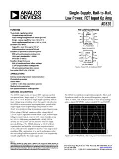
1 Semiconductor Components Industries, LLC, 2006 October, 2015 Rev. 101 Publication Order Number: MAX803 /DMAX803 Series,NCP803 SeriesVery Low Supply Current3-Pin Microprocessor Reset MonitorThe MAX803 /NCP803 is a cost effective system supervisor circuitdesigned to monitor VCC in digital systems and provide a reset signal tothe host processor when necessary. No external components reset output is driven active within 10 msec of VCC fallingthrough the reset voltage threshold. Reset is maintained active for atimeout period which is trimmed by the factory after VCC rises abovethe reset threshold. The MAX803 /NCP803 has an open drainactive low RESET output. Both devices are available in SOT 23 andSC 70 MAX803 /NCP803 is optimized to reject fast transient glitcheson the VCC line. Low Supply Current of mA (VCC = V) makethese devices suitable for battery powered Precision VCC Monitor for V, V, V, V, and VSupplies Precision Monitoring Voltages from V to V Availablein 100 mV Steps Four Guaranteed Minimum Power On Reset Pulse Width Available(1 ms, 20 ms, 100 ms, and 140 ms) RESET Output Guaranteed to VCC = V Low Supply Current VCC Transient Immunity No External Components Wide Operating Temperature: 40 C to 105 C These Devices are Pb Free and are RoHS CompliantTypical Applications Computers Embedded Systems Battery Powered Equipment Critical Microprocessor Power Supply MonitoringVCCVCCVCCRESETRESETMAX803 NCP803 GNDGNDF igure 1.
2 Typical Application DiagrammP00 Rpull upC = 100 nFSOT 23(TO 236)CASE 318 PIN CONFIGURATION312 VCCGNDRESETSOT 23/SC 70(Top View)MARKINGDIAGRAM321213xxx MGGxxx= Specific Device CodeM= Date CodeG= Pb Free Packagexx MGG1SC 70(SOT 323)CASE 419 See general marking information in the device markingsection on page 8 of this data MARKING INFORMATIONSee detailed ordering and shipping information in the packagedimensions section on page 8 of this data INFORMATION(Note: Microdot may be in either location) Series, NCP803 DESCRIPTIONPin 1 GND Ground 2 RESET RESET output remains low while VCC is below the reset voltage threshold, and for a reset timeoutperiod after VCC rises above reset threshold. 3 VCC Supply Voltage: C = 100 nF is recommended as a bypass capacitor between VCC and MAXIMUM RATINGSR atingSymbolValueUnitPower Supply Voltage (VCC to GND)VCC to Output Voltage (CMOS) to (VCC + )VInput Current , VCC20mAOutput Current , RESET20mAdV/dt (VCC)100V/msecThermal Resistance, Junction to Air (Note 1)SOT 23SC 70 RqJA301314 C/WOperating Junction Temperature RangeTJ 40 to +125 CStorage Temperature RangeTstg 65 to +150 CLead Temperature (Soldering, 10 Seconds)Tsol+260 CESD ProtectionHuman Body Model (HBM): Following Specification JESD22 A114 Machine Model (MM): Following Specification JESD22 A1152000200 VLatchup Current Maximum Rating.
3 Following Specification JESD78 Class IIPositiveNegativeILatchup200200mAStress es exceeding those listed in the Maximum Ratings table may damage the device. If any of these limits are exceeded, device functionalityshould not be assumed, damage may occur and reliability may be This based on a FR4 PCB with 10mm2 of 1 oz copper traces under natural convention conditions and a single The maximum package power dissipation limit must not be +TJ(max)*TARqJAwith TJ(max) = 150 CVref1 GND32 VCCRESETF igure 2. NCP803, MAX803 Series Open Drain Active Low OutputTimeoutCounterOscillatorMAX803 Series, NCP803 CHARACTERISTICS TA = 40 C to +105 C unless otherwise noted. Typical values are at TA = +25 C. (Note 3)CharacteristicSymbolMinTypMaxUnitVCC RangeTA = 0 C to +70 CTA = 40 C to +105 C (Note 4) CurrentVCC = VTA = 40 C to +85 CTA = 85 C to +105 C (Note 5)VCC = VTA = 40 C to +85 CTA = 85 C to +105 C (Note 5)ICC Threshold (Vin Decreasing) (Note 6)MAX803SQ463/NCP803SN463TA = +25 CTA = 40 C to +85 CTA = +85 C to +105 C (Note 5) = +25 CTA = 40 C to +85 CTA = +85 C to +105 C (Note 5) = +25 CTA = 40 C to +85 CTA = +85 C to +105 C (Note 5) = +25 CTA = 40 C to +85 CTA = +85 C to +105 C (Note 5) = +25 CTA = 40 C to +85 CTA = +85 C to +105 C (Note 5) = +25 CTA = 40 C to +85 CTA = +85 C to +105 C (Note 5) = +25 CTA = 40 C to +85 CTA = +85 C to +105 C (Note 5) = +25 CTA = 40 C to +85 CTA = +85 C to +105 C (Note 5) , MAX803SQ120TA = +25 CTA = 40 C to +85 CTA = +85 C to +105 C (Note 5)
4 Voltage Threshold Temperature Coefficient 30 ppm/ CVCC to Reset Delay VCC = VTH to (VTH 100 mV) 10 msecReset Active TimeOut Period (Note 6)MAX803SN(Q)293D1 MAX803SN(Q)293D2/MAX803SN(Q)308D2 MAX803SN(Q)293D3 MAX803SN(Q) Output Voltage LowVCC = VTH V v VTH v V, ISINK = V v VTH v V, ISINK = V v VTH v V, ISINK = mAVOL Leakage Current VCC u VTH, RESET De assertedILEAK 1mA3. Production testing done at TA = 25 C, over temperature limits guaranteed by For NCV automotive devices, this temperature range is TA = 40 C to +125 For NCV automotive devices, this temperature range is TA = +85 C to +125 Contact your ON Semiconductor sales representative for other threshold voltage and timeout Series, NCP803 40 C 40 CTYPICAL OPERATING 50 250255075 Supply VOLTAGE (V)TEMPERATURE ( C)Figure 3. Supply Current vs. Supply VOLTAGE (V) Supply Current (mA) Supply Current (mA) C25 C 40 C25 CVTH = VOLTAGE (V) C25 CSUPPLY Current (mA)VTH = VNORMALIZED THRESHOLD = V 50 25025500 TEMPERATURE ( C) Supply Current (mA) = VVCC = VVCC = VVTH = VVTH = VOLTAGE (V)OUTPUT VOLTAGE VCC (mV) 4.
5 Supply Current vs. Supply VoltageFigure 5. Supply Current vs. Supply VoltageFigure 6. Normalized Reset Threshold Voltagevs. TemperatureFigure 7. Supply Current vs. TemperatureFigure 8. Output Voltage Low vs. C25 C 40 CVTH = VISINK = 500 mARESET ASSERTEDMAX803 Series, NCP803 OPERATING CHARACTERISTICS7550250 50 2502550125 TEMPERATURE ( C)Figure 9. Power Down Reset Delay and Overdrive (VTH = V)300240180120600 TEMPERATURE ( C)POWER DOWN RESET DELAY (msec)POWER DOWN RESET DELAY (msec)100125 50 50 2502550100 TEMPERATURE ( C) POWER UP RESET TIMEOUTVOD = VCC VTHF igure 10. Power Down Reset Delay and Overdrive (VTH = V)Figure 11. Normalized Power Up Reset = 10 mVVOD = 20 mVVOD = 100 mVVOD = 200 mVVOD = VCC VTHVOD = 10 mVVOD = 20 mVVOD = 100 mVVOD = 200 Series, NCP803 Operation DescriptionThe MAX803 , NCP803 series microprocessor resetsupervisory circuits are designed to monitor the powersupplies in digital systems and provide a reset signal to theprocessor without any external components.
6 Figure 2 showsthe timing diagram and a typical application below. Initiallyconsider that input voltage VCC is at a nominal level greaterthan the voltage detector upper threshold (VTH). And theRESET(RESET) output voltage (Pin 2) will be in the highstate for MAX803 and NCP803 devices. If there is an inputpower interruption and VCC becomes significantlydeficient, it will fall below the lower detector threshold(VTH ). This event causes the RESET output to be in the lowstate for the MAX803 and NCP803 devices. Aftercompletion of the power interruption, VCC will rise to itsnominal level and become greater than the VTH. Thissequence activates the internal oscillator circuitry anddigital counter to count. After the count of the timeoutperiod, the reset output will revert back to the original +VTH VCCVTH 0 VVCCVTH 0 VInput VoltageReset OutputMAX803, NCP803 Reset OutputMAX810 Figure 12.
7 Timing WaveformsMAX803 Series, NCP803 INFORMATIONVCC Transient RejectionThe MAX803 /NCP803 series provides accurate VCCmonitoring and reset timing during power up,power down, and brownout/sag conditions, and rejectsnegative going transients (glitches) on the power supplyline. Figure 13 shows the maximum transient duration negative excursion (overdrive) for glitchrejection. Any combination of duration and overdrive whichlies under the curve will not generate a reset above the curve are detected as a brownout orpower down. Typically, transient that goes 100 mV belowthe reset threshold and lasts ms or less will not cause areset pulse. Transient immunity can be improved by addinga capacitor in close proximity to the VCC pin of 13. Maximum Transient Duration for Glitch Rejection at 25 CDurationVTHO verdriveVCC1025020011060 MAXIMUM TRANSIENT DURATION (msec)50 RESET COMPARATOR OVERDRIVE (mV)0410150100 VTH = V160210260310360 VTH = VRESET Signal Integrity During Power DownThe MAX803 /NCP803 RESET output is valid to VCC = V.
8 Below this voltage the output becomes an opencircuit and does not sink Current . This means CMOS logicinputs to the Microprocessor will be floating at anundetermined voltage. Most digital systems are completelyshutdown well above this voltage. However, in situationswhere RESET must be maintained valid to VCC = 0 V, sincethe NCP803/ MAX803 has Open Drain and active lowoutput, it typically uses a pullup resistor. With this device,RESET will most likely not maintain an active condition,but will drift to a non active level due to the pullup resistorand the reduced sinking capability of the open drain , this device is not recommended for applicationswhere the RESET pin is required to be valid down toVCC = 0 k*MAX809 NCP803 GNDF igure 14. RESET Signal IntegrityRESET*Assume High Z Reset Input to MicroprocessorMAX803 RESET Output Allows Use With Two PowerSuppliesIn numerous applications the pullup resistor place on theRESET output is connected to the Supply voltage monitoredby the IC.
9 Nevertheless, a different Supply voltage can alsopower this output and so level shift from the monitoredsupply to reset the microprocessor. However, if theNCP803/ MAX803 s Supply goes blew 1 V, the RESET output ability to sink Current will decrease and the result isa high state on the pin even though the Supply s IC is underthe threshold level. This occurs at a VCC level that dependson the Rpullup value and the voltage which is 15. MAX803 RESET Output with Two SuppliesRESETVCCVCC1 MAX803 Series, NCP803 , MARKING AND THRESHOLD INFORMATIONPart NumberVth**(V)Time out**(ms)DescriptionMarkingPackageShippi ng 460 Open Drain RESETSCQSOT23 3(Pb Free)3000 / Tape & 460 SQRSOT23 3(Pb Free) 460 SQCSOT23 3(Pb Free) 460 SQDSOT23 3(Pb Free) 460 SQESOT23 3(Pb Free) 460 RADSOT23 3(Pb Free) 460 SQFSOT23 3(Pb Free) 460 SQGSOT23 3(Pb Free) 460 SSWSOT23 3(Pb Free) 3(Pb Free) 66 SSYSOT23 3(Pb Free) 330 SSZSOT23 3(Pb Free) 460 ZVSC70 3(Pb Free) 460 SXSC70 3(Pb Free) 460 ZWSC70 3(Pb Free) 460 ZXSC70 3(Pb Free)NCV803SQ308T1G*140 460 ZYSC70 3(Pb Free) 460 ZZSC70 3(Pb Free) 3(Pb Free) 66 YBSC70 3(Pb Free) 66 SYSC70 3(Pb Free)NCV803SQ308D2T1G*20 330 YCSC70 3(Pb Free) 460 SQDSOT23 3(Pb Free)
10 10000 / Tape &Reel For information on tape and reel specifications, including part orientation and tape sizes, please refer to our Tape and Reel PackagingSpecifications Brochure, BRD8011/D.*NCV Prefix for Automotive and Other Applications Requiring Unique Site and Control Change Requirements; AEC Q100 Qualified and PPAPC apable.**Contact your ON Semiconductor sales representative for other threshold voltage options.**Contact your ON Semiconductor sales representative for timeout options availability for other threshold voltage 23 (TO 236)CASE 318 08 ISSUE ASDATE 30 JAN 2018 SCALE 4:1DA13121 XXXMGGXXX = Specific Device CodeM= Date CodeG= Pb Free Package*This information is generic. Please refer todevice data sheet for actual part Free indicator, G or microdot G ,may or may not be DIAGRAM*NOTES:1. DIMENSIONING AND TOLERANCING PER ASME , CONTROLLING DIMENSION: MAXIMUM LEAD THICKNESS INCLUDES LEAD LEAD THICKNESS IS THE MINIMUM THICKNESS OFTHE BASE DIMENSIONS D AND E DO NOT INCLUDE MOLD FLASH,PROTRUSIONS, OR GATE FOOTPRINTVIEW VIEW 22:PIN 1.