Transcription of MC74HC165A - 8-Bit Serial or Parallel-Input/Serial-Output ...
1 Semiconductor Components Industries, LLC, 2014 March, 2020 Rev. 101 Publication Order Number: MC74HC165A /D8-Bit Serial orParallel- input / Serial - output Shift RegisterHigh Performance Silicon Gate CMOSMC74HC165 AThe MC74HC165A is identical in pinout to the LS165. The deviceinputs are compatible with standard CMOS outputs; with pullupresistors, they are compatible with LSTTL device is an 8 bit shift register with complementary outputsfrom the last stage. Data may be loaded into the register either inparallel or in Serial form. When the Serial Shift/ parallel Load input islow, the data is loaded asynchronously in parallel . When the SerialShift/ parallel Load input is high, the data is loaded serially on therising edge of either Clock or Clock Inhibit (see the Function Table).
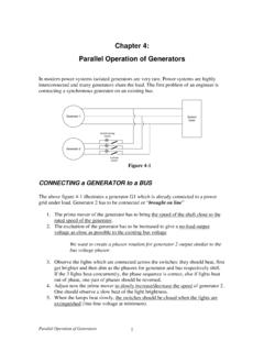
2 The 2 input NOR clock may be used either by combining twoindependent clock sources or by designating one of the clock inputs toact as a clock output Drive Capability: 10 LSTTL Loads Outputs Directly Interface to CMOS, NMOS, and TTL Operating Voltage Range: to V Low input Current: 1 mA High Noise Immunity Characteristic of CMOS Devices In Compliance with the Requirements Defined by JEDEC StandardNo. 7 A Chip Complexity: 286 FETs or Equivalent Gates NLV Prefix for Automotive and Other Applications RequiringUnique Site and Control Change Requirements; AEC Q100 Qualified and PPAP Capable These Devices are Pb Free, Halogen Free and are RoHS CompliantSee detailed ordering and shipping information in the packagedimensions section on page 6 of this data INFORMATIONMARKINGDIAGRAMSSOIC 16D SUFFIXCASE 751 BTSSOP 16DT SUFFIXCASE 948F116 PDIP 16N SUFFIXCASE 648116116116MC74HC165 ANAWLYYWWG116HC165 AGAWLYWWHC165 AALYWGG116A= Assembly LocationL, WL= Wafer LotY, YY= YearW, WW= Work WeekG or G= Pb Free Package(Note: Microdot may be in either location)165 AALYWGGQFN16MN SUFFIXCASE 16 = VCCPIN 8 = GND11121314345610 ABCDEFGHSAPARALLELDATAINPUTSSERIALDATAIN PUTSERIAL SHIFT/ parallel LOAD1215 CLOCKCLOCK INHIBIT97 QHQHSERIALDATAOUTPUTSF igure 1.
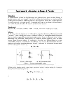
3 Pin Assignments13141516910111254321876 BCDCLOCK INHIBITVCCQHSAAFECLOCKSERIAL SHIFT/ parallel LOADGNDQHHGF igure 2. Logic Diagram11621531441351261171089 GNDBCDCLOCK INHIBITVCCQHSAAFECLOCKSERIAL SHIFT/ parallel LOADGNDQHHGFUNCTION TABLEI nputsInternal StagesOutputOperationSerial Shift/ parallel LoadClockClockInhibitSAA HQAQBQHLXXXa .. habhAsynchronous parallel LoadHHLLLHXXLHQAnQAnQGnQGnSerial Shift via ClockHHLLLHXXLHQAnQAnQGnQGnSerial Shift via Clock InhibitHHXHHXXXXXNo ChangeInhibited ClockHLLXXNo ChangeNo ClockX = don t careQAn QGn = Data shifted from the preceding RATINGSS ymbolParameterValueUnitVCCDC Supply Voltage (Referenced to GND) to + input Voltage (Referenced to GND) to VCC + output Voltage (Referenced to GND) to VCC + input Current, per Pin 20mAIoutDC output Current, per Pin 25mAICCDC Supply Current, VCC and GND Pins 50mAPDP ower Dissipation in Still AirPlastic DIP SOIC Package TSSOP Package 750500450mWTstgStorage Temperature 65 to + 150_CTLLead Temperature, 1 mm from Case for 10 Seconds(Plastic DIP, SOIC or TSSOP Package)
4 260_CStresses exceeding those listed in the Maximum Ratings table may damage the device. If any ofthese limits are exceeded, device functionality should not be assumed, damage may occur andreliability may be affected. Derating Plastic DIP: 10 mW/_C from 65_ to 125_CSOIC Package: 7 mW/_C from 65_ to 125_CTSSOP Package: mW/_C from 65_ to 125_CRECOMMENDED OPERATING CONDITIONSS ymbolParameterMinMaxUnitVCCDC Supply Voltage (Referenced to GND) , VoutDC input Voltage, output Voltage (Referenced toGND)0 VCCVTAO perating Temperature, All Package Types 55+ 125_Ctr, tfInput Rise and Fall TimeVCC = V(Figure 1)VCC = VVCC = VVCC = V0001000600500400nsFunctional operation above the stresses listed in the Recommended Operating Ranges is notimplied. Extended exposure to stresses beyond the Recommended Operating Ranges limits mayaffect device ELECTRICAL CHARACTERISTICS (Voltages Referenced to GND)SymbolParameterTest ConditionsVCCVG uaranteed LimitUnit 55 to 25_Cv 85_Cv 125_CVIHM inimum High Level InputVoltageVout = V or VCC V|Iout| v 20 Low Level InputVoltageVout = V or VCC V|Iout| v 20 High Level OutputVoltageVin = VIH or VIL|Iout| v 20 = VIH or VIL|Iout| v mA|Iout| v mA|Iout| v device contains protectioncircuitry to guard against damagedue to high static voltages or electricfields.
5 However, precautions mustbe taken to avoid applications of anyvoltage higher than maximum ratedvoltages to this high impedance cir-cuit. For proper operation, Vin andVout should be constrained to therange GND v (Vin or Vout) v inputs must always betied to an appropriate logic voltagelevel ( , either GND or VCC).Unused outputs must be left ELECTRICAL CHARACTERISTICS (Voltages Referenced to GND)Guaranteed LimitVCCS ymbolUnitv 125_Cv 85_C 55 to 25_CVCCVTest ConditionsParameterVOLM aximum Low Level OutputVoltageVin = VIH or VIL|Iout| v 20 = VIH or VIL|Iout| v mA|Iout| v mA|Iout| v input LeakageCurrentVin = VCC or Quiescent SupplyCurrent (per Package)Vin = VCC or GNDIout = 0 parametric performance is indicated in the Electrical Characteristics for the listed test conditions, unless otherwise noted.
6 Productperformance may not be indicated by the Electrical Characteristics if operated under different ELECTRICAL CHARACTERISTICS (CL = 50 pF, input tr = tf = 6 ns)SymbolParameterVCCVG uaranteed LimitUnit 55 to 25_Cv 85_Cv 125_CfmaxMaximum Clock Frequency (50% Duty Cycle)(Figures 1 and 8) ,tPHLM aximum Propagation Delay, Clock (or Clock Inhibit) to QH or QH(Figures 1 and 8) ,tPHLM aximum Propagation Delay, Serial Shift/ parallel Load to QH or QH(Figures 2 and 8) ,tPHLM aximum Propagation Delay, input H to QH or QH(Figures 3 and 8) ,tTHLM aximum output Transition Time, Any output (Figures 1 and 8) input Capacitance 101010pFCPDP ower Dissipation Capacitance (Per Package)*Typical @ 25 C, VCC = VpF40* Used to determine the no load dynamic power consumption: PD = CPD VCC2f + ICC REQUIREMENTS ( input tr = tf = 6 ns)SymbolParameterVCCVG uaranteed LimitUnit 55 to 25_Cv 85_Cv 125_CtsuMinimum Setup Time, parallel Data Inputs to Serial Shift/ parallel Load(Figure 4) Setup Time, input SA to Clock (or Clock Inhibit)(Figure 5) Setup Time, Serial Shift/ parallel Load to Clock (or Clock Inhibit)(Figure 6) Setup Time, Clock to Clock Inhibit(Figure 7) Hold Time, Serial Shift/ parallel Load to parallel Data Inputs(Figure 4) Hold Time, Clock (or Clock Inhibit) to input SA(Figure 5) Hold Time, Clock (or Clock Inhibit) to Serial Shift/ parallel Load(Figure 6) Recovery Time, Clock to Clock Inhibit(Figure 7) Pulse Width, Clock (or Clock Inhibit)(Figure 1) Pulse width, Serial Shift/ parallel Load(Figure 2)
7 , tfMaximum input Rise and Fall Times(Figure 1) DESCRIPTIONSINPUTSA, B, C, D, E, F, G, H (Pins 11, 12, 13, 14, 3, 4, 5, 6) parallel Data inputs. Data on these inputs areasynchronously entered in parallel into the internalflip flops when the Serial Shift/ parallel Load input is (Pin 10) Serial Data input . When the Serial Shift/ parallel Loadinput is high, data on this pin is serially entered into the firststage of the shift register with the rising edge of the INPUTSS erial Shift/ parallel Load (Pin 1)Data entry control input . When a high level is applied tothis pin, data at the Serial Data input (SA) are shifted into theregister with the rising edge of the Clock. When a low levelis applied to this pin, data at the parallel Data inputs areasynchronously loaded into each of the eight internal , Clock Inhibit (Pins 2, 15)Clock inputs.
8 These two clock inputs function may be used as an active high clock , to avoid double clocking, the inhibit input shouldgo high only while the clock input is shift register is completely static, allowing Clockrates down to DC in a continuous or intermittent , QH (Pins 9, 7)Complementary Shift Register outputs. These pins are thenoninverted and inverted outputs of the eighth stage of theshift INFORMATIOND evicePackageShipping MC74HC165 ANGPDIP 16(Pb Free)500 Units / RailMC74HC165 ADGSOIC 16(Pb Free)48 Units / RailMC74HC165 ADR2G2500 Units / ReelNLV74HC165 ADR2G*2500 Units / ReelMC74HC165 ADTR2 GTSSOP 16(Pb Free)2500 Units / ReelNLV74HC165 ADTR2G*2500 Units / ReelMC74HC165 AMNTWGQFN16(Pb Free)3000 Units / ReelMC74HC165 AMN2 TWG3000 Units / Reel For information on tape and reel specifications, including part orientation and tape sizes, please refer to our Tape and Reel PackagingSpecifications Brochure, BRD8011/D.
9 *NLV Prefix for Automotive and Other Applications Requiring Unique Site and Control Change Requirements; AEC Q100 Qualified and WAVEFORMS trtfVCCGND90%50%10%tPLHtPHLCLOCKOR CLOCK INHIBIT90%50%10%tTLHtTHLQH OR QHSERIAL SHIFT/ parallel LOADQH OR QH50%tPLH50%VCCGNDtPHL50%trtfINPUT H90%50%10%90%50%10%VCCGNDtPHLtTHLtTLHtPL HQH OR QH50%VCCGNDthVCCGNDASYNCHRONOUS PARALLELLOAD(LEVEL SENSITIVE) Serial SHIFT/ parallel LOADINPUTS A-HINPUT SA50%50%CLOCKOR CLOCK INHIBITVCCGNDVCCGNDSERIAL SHIFT/ parallel LOADCLOCKOR CLOCK INHIBIT50%50%tsuVCCGNDVCCGNDCLOCK 2 INHIBITEDCLOCK INHIBITCLOCK50%50%tsutrecVCCGNDVCCGND*In cludes all probe and jig capacitanceCL*TEST POINTDEVICEUNDERTESTOUTPUTtw1/fmaxtwVALI DtsuVALID tsuththFigure 3. Serial Shirt ModeFigure 4. parallel Load ModeFigure 5. parallel Load ModeFigure 6.
10 parallel Load ModeFigure 7. Serial Shift ModeFigure 8. Serial Shift ModeFigure 9. Serial Shift, Clock Inhibit ModeFigure 10. Test FGH1112134569QH7 QHSERIAL SHIFT/ parallel LOAD1 Serial DATAINPUT SA10 CLOCK2 CLOCKINHIBIT15 EXPANDED LOGIC DIAGRAMCLOCKCLOCK INHIBITSASERIAL SHIFT/ parallel LOADABCDEFGHQHQHHLHLHLHHHHLLLHHLLHHLLHHL parallel LOADPARALLELDATAINPUTSTIMING DIAGRAMDQACCDQBCCDQCCCDQFCCDQGCCDQHCCCLO CKINHIBITMODESERIAL-SHIFT MODEQFN16, , 485AW 01 ISSUE ODATE 11 DEC 2008 DIM :1. DIMENSIONING AND TOLERANCING PERASME , CONTROLLING DIMENSION: DIMENSIONS b APPLIES TO PLATEDTERMINAL AND IS MEASURED AND MM FROM COPLANARITY APPLIES TO THE EXPOSEDPAD AS WELL AS THE REFbD2 LPIN ONE 3A16 XKA1(A3) 2:1 GENERIC MARKINGDIAGRAM*XXXX= Specific Device CodeA= Assembly LocationL= Wafer LotY= YearW= Work WeekG= Pb Free PackageXXXXALYWGG1*This information is generic.