Transcription of 3.5 GSPS Direct Digital Synthesizer with 12-Bit DAC …
1 GSPS Direct Digital Synthesizer with 12-Bit DACData Sheet ad9914 Rev. F Document Feedback Information furnished by Analog Devices is believed to be accurate and reliable. However, no responsibility is assumed by Analog Devices for its use, nor for any infringements of patents or other rights of third parties that may result from its use. Specifications subject to change without notice. No license is granted by implication or otherwise under any patent or patent rights of Analog Devices. Trademarks and registered trademarks are the property of their respective owners.
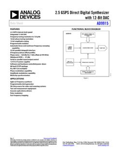
2 One Technology Way, Box 9106, Norwood, MA 02062-9106, : 2012 2016 Analog Devices, Inc. All rights reserved. Technical Support FEATURES GSPS internal clock speed Integrated 12-Bit DAC Frequency tuning resolution to 190 pHz 16-bit phase tuning resolution 12-Bit amplitude scaling Programmable modulus Automatic linear and nonlinear frequency sweeping capability 32-bit parallel datapath interface 8 frequency/phase offset profiles Phase noise: 128 dBc/Hz (1 kHz offset at 1396 MHz) Wideband SFDR < 50 dBc Serial or parallel input/output control V power supplies Software and hardware controlled power-down 88-lead LFCSP package PLL REF CLK multiplier Phase modulation capability Amplitude modulation capability APPLICATIONS Agile LO frequency synthesis Programmable clock generator FM chirp source for radar and scanning systems Test and measurement equipment Acousto-optic device drivers Polar modulator Fast frequency hopping FUNCTIONAL BLOCK DIAGRAM 12-Bit DDS CORETIMING AND CONTROL10836-001AD9914 HIGH SPEED
3 PARALLELMODULATIONPORTLINEARSWEEPBLOCKSE RIAL OR PARALLELDATA PORTREF CLKMULTIPLIER Figure 1. ad9914 Data Sheet Rev. F | Page 2 of 45 TABLE OF CONTENTS Features .. 1 Applications .. 1 Functional Block Diagram .. 1 Revision History .. 2 General Description .. 3 Specifications .. 4 DC Specifications .. 4 AC Specifications .. 5 Absolute Maximum Ratings .. 8 Thermal Performance .. 8 ESD Caution .. 8 Pin Configuration and Function Descriptions .. 9 Typical Performance Characteristics .. 12 Equivalent Circuits .. 16 Theory of Operation .. 17 Single Tone Mode.
4 17 Profile Modulation Mode .. 17 Digital Ramp Modulation Mode .. 17 Parallel Data Port Modulation Mode .. 17 Programmable Modulus Mode .. 17 Mode Priority .. 18 Functional Block Detail .. 19 DDS Core .. 19 12-Bit DAC Output .. 20 DAC Calibration Output .. 20 Reconstruction Filter .. 20 Clock Input (REF_CLK/REF_CLK) .. 21 PLL Lock Indication .. 22 Output Shift Keying (OSK) .. 22 Digital Ramp Generator (DRG) .. 23 Power-Down Control .. 27 Programming and Function Pins .. 28 Serial Programming .. 31 Control Interface Serial Input/Output .. 31 General Serial Input/Output Operation.
5 31 Instruction Byte .. 31 Serial Input/Output Port Pin Descriptions .. 31 Serial Input/Output Timing Diagrams .. 32 MSB/LSB Transfers .. 32 Parallel Programming (8-/16-Bit) .. 33 Register Map and Bit Descriptions .. 34 Register Bit Descriptions .. 39 Outline Dimensions .. 45 Ordering Guide .. 45 REVISION HISTORY 6/2016 Rev. E to Rev. F Changes to Figure 19 .. 14 1/2016 Rev. D to Rev. E Changes to DDS Core Section .. 19 Change to Figure 30 .. 19 Updated Outline Dimensions .. 45 1/2014 Rev. C to Rev. D Changes to Digital Timing Specifications Parameter, Table 2.
6 5 Changes to Figure 23 .. 15 Change to DAC Calibration Output Section .. 20 Change to Address 0x02, Table 14 .. 34 Changes to Table 17 .. 41 11/2013 Rev. B to Rev. C Changes to Table 2 .. 5 Change to Programming and Function Pins Section .. 30 7/2013 Rev. A to Rev. B Change to CMOS Logic Outputs Parameter, Table 1 .. 4 Changes to Table 2 .. 7 Changes to DDS Core Section .. 19 Changes to Phase-Locked Loop (PLL) Multiplier Section .. 21 Changed PLL Charge Pump Section to PLL Charge Pump/ Total Feedback Divider Section; Changes to Table 8, PLL Loop Filter Components Section, and Figure 34.
7 22 Change to Table 14 .. 34 Changes to Bits [15:8], Table 17 .. 42 8/2012 Rev. 0 to Rev. A Changes to Features Section .. 1 Changed Differential Input Voltage Unit from mV p-p to V p-p .. 4 Changes to Table 14 .. 34 Changes to Table 16 .. 40 Changes to Table 28 .. 44 Updated Outline Dimensions .. 45 7/2012 Revision 0: Initial Version Data Sheet ad9914 Rev. F | Page 3 of 45 GENERAL DESCRIPTION The ad9914 is a Direct Digital Synthesizer (DDS) featuring a 12-Bit DAC. The ad9914 uses advanced DDS technology, coupled with an internal high speed, high performance DAC to form a digitally programmable, complete high frequency Synthesizer capable of generating a frequency-agile analog output sinusoidal waveform at up to GHz.
8 The ad9914 enables fast frequency hopping and fine tuning resolution (64-bit capable using programmable modulus mode). The ad9914 also offers fast phase and amplitude hopping capability. The frequency tuning and control words are loaded into the ad9914 via a serial or parallel input/output port. The ad9914 also supports a user defined linear sweep mode of operation for generating linear swept waveforms of frequency, phase, or amplitude. A high speed, 32-bit parallel data input port is included, enabling high data rates for polar modulation schemes and fast reprogramming of the phase, frequency, and amplitude tuning words.
9 The ad9914 is specified to operate over the extended industrial temperature range (see the Absolute Maximum Ratings section). 10836-00232F0 TO F3D0 TO D31PS[2:0]I/O_UPDATEPOWER-DOWNCONTROLEXT _PWR_DWNDAC_RSETAOUTAOUTOSKDROVERDRCTLDR HOLDSYNC_CLKA CLOCKAMPLITUDE (A)FREQUENCY ( )PHASE ( )DIGITALRAMPGENERATOR24 MULTICHIPSYNCHRONIZATIONSYSCLKPLLREF_CLK REF_CLKAD9914 OUTPUTSHIFTKEYINGDATAROUTEANDPARTITIONCO NTROL3 INTERNAL CLOCK TIMINGAND CONTROL Acos ( t + )Asin ( t + )SYNC_OUTSYNC_INLOOP_FILTERMASTER_RESETD AC12-BITDDSINTERNALPROGRAMMINGREGISTERS Figure 2.
10 Detailed Block Diagram ad9914 Data Sheet Rev. F | Page 4 of 45 SPECIFICATIONS DC SPECIFICATIONS AVDD ( V) and DVDD ( V) = V 5%, AVDD ( V) and DVDD_I/O ( V) = V 5%, TA = 25 C, RSET = k , IOUT = 20 mA, external reference clock frequency = GHz with reference clock (REF CLK) multiplier bypassed, unless otherwise noted. Table 1. Parameter Min Typ Max Unit Test Conditions/Comments SUPPLY VOLTAGE DVDD_I/O V Pin 16, Pin 83 DVDD V Pin 6, Pin 23, Pin 73 AVDD ( V) V Pin 34, Pin 36, Pin 39, Pin 40, Pin 43, Pin 47, Pin 50, Pin 52, Pin 53, Pin 60 AVDD ( V) V Pin 32, Pin 56, Pin 57 SUPPLY CURRENT See also the total power dissipation specifications IDVDD_I/O 20 mA Pin 16, Pin 83 IDVDD 433 mA Pin 6, Pin 23, Pin 73 IAVDD( ) 640 mA Pin 34, Pin 36, Pin 39, Pin 40, Pin 43, Pin 47, Pin 50, Pin 52, Pin 53, Pin 60 IAVDD( )