Transcription of AN-5086 - USB Type-C, CC Pin Design Considerations
1 Semiconductor Components Industries, LLC, 2016 September, 2017 Rev. 21 Publication Order Number:AN 5086/DAN-5086/DUSB Type-C, CC Pin DesignConsiderationsHigh voltage Design Considerations forType C connector pins in systemssupporting non-USB standard chargingprotocol and/or fault casesSUMMARYWhen designing hardware systems with Type Cconnectors, a designer also has to consider all legacy,standard, and non-standard specifications that exist in theUSB connector eco system. With the introduction of theType C connector and the Configuration channel (CC Pin)new challenges occur trying to ensure overall systemrobustness.
2 This note addresses some of the concerns withthe CC pin in a robust system Considerations SYSTEM ESD AND SURGEIEC61000 4 2 (henceforth called just IEC ) is theindustry s standard for system level ESD testing. IEC testingis a system level test, while other ESD specifications likeCharged Device Model (CDM) and Human Body Model(HBM) target the manufacturing process and humanhandling. Most IC s have integrated Electro-StaticDischarge (ESD) protection intended to protect the deviceduring manufacturing while external protection in the formof a TVS is added for the IEC system level testing.
3 It is veryimportant to understand that, implementing TVS protectionat the system level and having it work together with theindividual IC, is the best way to achieve overall are few important specifications to ensure the rightTVS is selected based on the Type C specification, and theType C controller ESD Standoff VoltageThis specification is important spec to look at whenselecting a TVS, due to the types of signals that will utilizethe CC pin during normal operation, as well as absolutemaximum spec. of the CC controller IC. Selecting the rightvalue ensures the TVS is actually effective in protecting thesystem.
4 Reverse Standoff Voltage, VRWM, is a commonspecification in a TVS product data sheet. For the CC pin, weshould pick a 5 V maximum for the VRWM, due to normaloperation of the CC pin, there should never be a case wherethe CC pin should exceed 5 V, and also the reverse standoffvoltage should be lower than the absolute maximum voltageon the CC controller CapacitanceIn Power Delivery specification, section , BMCreceiver capacitance requirements are shown below inTable 1. BCM RECEIVER NORMATIVE REQUIREMENTS NameDescriptionMinNomMaxUnitCommentcRece iverCC ReceiverCapacitance200 600pFThe DFP or UFP system shall have capacitance within thisrange when not transmitting on the lineThe cReceiver requirement of the CC receivercapacitance is 200 pF to 600 pF, this has a direct impact onPD communication.
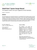
5 Any device in the CC path, such asa TVS diode, needs to ensure that capacitance of the devicedoes not exceed this specification but can also be used tomeet the minimum capacitance requirements. By choosingthe appropriate TVS that works well in the system, you canavoid placing additional capacitance on the CC line byutilizing just the diode VoltageBreakdown voltage is the voltage threshold where theTVS diode becomes more conductive to ground and allowshigher amount of current flow from cathode to 1 shows a typical TVS I V cure, and as we can seeafter the VBR, the current shot up very quickly as the TVSbecame very conductive.
6 The voltage increases until it hitsthe clamping voltage where the TVS effectively becomesa resistor that shorts to ground. With a large amount NOTEAN 5086 passing though the TVS, it will eventually burn upand destroy the diode in this clamped 1. TVS I V CurveIn order to make sure proper function of the Type C CCline communication, and overall system are protected inESD/Surge event, the correct breakdown voltage must beconsidered. In Type C Design , the CC pin break downvoltage should be above 5 V to ensure normal operation, andbelow 7 V to ensure that the TVS can help direct extracharge to ground when fault CONSIDERATION NONE USBSTANDARD CHARGING PROTOCOLS tandard spec.
7 Of 500 mA charging current isclearly not enough for the majority of the devices in themarket today, power/process intensive devices such asmobile phones have implemented higher than charging protocol to allow for shorter and fastercharging. Due to the limitation of the USB cable it is notideal to push more than A of current. In order to be ableto charge at higher wattage, non-Type C connector baseddesigns have gone above 5 V on VBUS to reduce chargingtime of the device. Due to backward compatibility supportof Type C, the Type C specification allows legacy adapterslike a Type A to Type C Cable.
8 The Type A to Type C andType C to USB mB cable integrate an internal pull upresistor (Rp) in the cable. Below is a functional model in thespecification 2. Legacy Host Port to DRP Functional ModelAN 5086 this case when the non-standard USB charging protocolincreases the VBUS voltage level, the CC pin will also bepulled up due to Rp. When following the Type Cspecification, the Rp value should be 56 kW, which meansthere will be two cases of higher than normal voltage presenton the CC 1 Rd is EnabledWe can simply calculate the voltage that will show up onthe CC line with Equation +VBUS (eq.)
9 1)Assume Rd = kW, Rp = 56 kWIn Table 2 we can find the typical VBUS voltage ofnon-standard charging protocol and its corresponding 2. VBUS TO CC VOLTAGE WHEN Rd ENABLEDVBUSVCC9 V12 V15 V20 VTable 2 shows that voltage on CC line is still relativelylow, so there is no high voltage concern for this 2 Rd is DisabledWith Rd disabled, the CC line will be pulled high to VBUS voltage, so in this case high voltage will show up on the CCline, thus protection is needed. However, since the current islimited by the 56 kW we can uses the Zener diode to clampthe voltage down. We will discuss how to select the correctZener in the next section.
10 If the proper Zener diode isselected, it can also protect against Illegal Type A toType C cables with incorrect 3 Rapid Insert and Removal of CableSome non-standard USB legacy chargers achieve fastercharging time by increasing the VBUS voltage. In certaincases, when a user unplugs the device from the charger/hostadapter and cable, while the system is charging at higherthan 5 V, there will be a short time period for the charger torecognize disconnect event and disable the VBUS this time, if the Rp is still connected to VBUS, andsince it is no longer connected to the device, the residualcharge will bring the CC pin to the same voltage as VBUS andslowly discharge over time.