Transcription of DTA144E - Digital Transistors (BRT), R1 = 47 kΩ, R2 = 47 kΩ
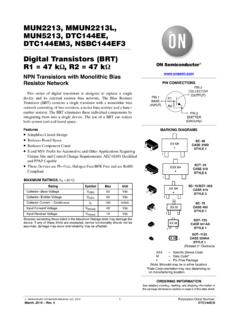
1 Semiconductor Components Industries, LLC, 2012 October, 2016 Rev. 51 Publication Order Number: DTA144E /DMUN2113, MMUN2113L,MUN5113, DTA144EE,DTA144EM3, NSBA144EF3 Digital Transistors (BRT)R1 = 47 kW, R2 = 47 kWPNP Transistors with Monolithic BiasResistor NetworkThis series of Digital Transistors is designed to replace a singledevice and its external resistor bias network. The Bias ResistorTransistor (BRT) contains a single transistor with a monolithic biasnetwork consisting of two resistors; a series base resistor and a base emitter resistor. The BRT eliminates these individual components byintegrating them into a single device.
2 The use of a BRT can reduceboth system cost and board Simplifies Circuit Design Reduces Board Space Reduces Component Count S and NSV Prefix for Automotive and Other Applications RequiringUnique Site and Control Change Requirements; AEC-Q101 Qualifiedand PPAP Capable These Devices are Pb Free, Halogen Free/BFR Free and are RoHSCompliantMAXIMUM RATINGS (TA = 25 C)RatingSymbolMaxUnitCollector Base VoltageVCBO50 VdcCollector Emitter VoltageVCEO50 VdcCollector Current ContinuousIC100mAdcInput Forward VoltageVIN(fwd)40 VdcInput Reverse VoltageVIN(rev)10 VdcStresses exceeding those listed in the Maximum Ratings table may damage thedevice.
3 If any of these limits are exceeded, device functionality should not beassumed, damage may occur and reliability may be 3 COLLECTOR(OUTPUT)PIN 2 EMITTER(GROUND)PIN 1 BASE(INPUT)R1R2 See detailed ordering, marking, and shipping information inthe package dimensions section on page 2 of this data 75 CASE 463 STYLE 1 MARKING DIAGRAMSXXX= Specific Device CodeM= Date Code*G=Pb Free Package(Note: Microdot may be in either location)*Date Code orientation may vary depending up-on manufacturing 59 CASE 318 DSTYLE 1 SOT 23 CASE 318 STYLE 6SC 70/SOT 323 CASE 419 STYLE 3 SOT 723 CASE 631 AASTYLE 1 SOT 1123 CASE 524 AASTYLE 1XX MGG11 XXX MGGXX MGG1XX M1X MXX M11 PIN CONNECTIONSMUN2113, MMUN2113L, MUN5113, DTA144EE, DTA144EM3, 1.
4 ORDERING INFORMATIOND evicePart MarkingPackageShipping MUN2113T1G, SMUN2113T1G*6 CSC 59(Pb Free)3000 / Tape & ReelMMUN2113LT1G, SMMUN2113LT1G*A6 CSOT 23(Pb Free)3000 / Tape & ReelMMUN2113LT3G, NSVMMUN2113LT3G*A6 CSOT 23(Pb Free)10000 / Tape & ReelMUN5113T1G, SMUN5113T1G*6 CSC 70/SOT 323(Pb Free)3000 / Tape & ReelMUN5113T3G6 CSC 70/SOT 323(Pb Free)10000 / Tape & ReelDTA144 EET1G, NSVDTA144 EET1G*6 CSC 75(Pb Free)3000 / Tape & ReelDTA144EM3T5G6 CSOT 723(Pb Free)8000 / Tape & ReelNSBA144EF3T5 GESOT 1123(Pb Free)8000 / Tape & Reel For information on tape and reel specifications, including part orientation and tape sizes, please refer to our Tape and Reel PackagingSpecifications Brochure, BRD8011 1.
5 Derating CurveAMBIENT TEMPERATURE ( C)1251007550250 25 50050100150200250300PD, POWER DISSIPATION (mW)150(1) (2) (3) (4) (5)(1) SC 75 and SC 70/SOT 323; Minimum Pad(2) SC 59; Minimum Pad(3) SOT 23; Minimum Pad(4) SOT 1123; 100 mm2, 1 oz. copper trace(5) SOT 723; Minimum PadMUN2113, MMUN2113L, MUN5113, DTA144EE, DTA144EM3, 2. THERMAL CHARACTERISTICSC haracteristicSymbolMaxUnitTHERMAL CHARACTERISTICS (SC 59) (MUN2113)Total Device DissipationTA = 25 C(Note 1)(Note 2)Derate above 25 C(Note 1)(Note 2) CThermal Resistance,(Note 1)Junction to Ambient(Note 2)RqJA540370 C/WThermal Resistance,(Note 1)Junction to Lead (Note 2)RqJL264287 C/WJunction and Storage Temperature RangeTJ, Tstg 55 to +150 CTHERMAL CHARACTERISTICS (SOT 23) (MMUN2113L)Total Device DissipationTA = 25 C(Note 1)(Note 2)Derate above 25 C(Note 1)(Note 2) CThermal Resistance,(Note 1)Junction to Ambient(Note 2)RqJA508311 C/WThermal Resistance,(Note 1)
6 Junction to Lead (Note 2)RqJL174208 C/WJunction and Storage Temperature RangeTJ, Tstg 55 to +150 CTHERMAL CHARACTERISTICS (SC 70/SOT 323) (MUN5113)Total Device DissipationTA = 25 C(Note 1)(Note 2)Derate above 25 C(Note 1)(Note 2) CThermal Resistance,(Note 1)Junction to Ambient(Note 2)RqJA618403 C/WThermal Resistance,(Note 1)Junction to Lead (Note 2)RqJL280332 C/WJunction and Storage Temperature RangeTJ, Tstg 55 to +150 CTHERMAL CHARACTERISTICS (SC 75) (DTA144EE)Total Device DissipationTA = 25 C(Note 1)(Note 2)Derate above 25 C(Note 1)(Note 2) CThermal Resistance,(Note 1)Junction to Ambient(Note 2)RqJA600400 C/WJunction and Storage Temperature RangeTJ, Tstg 55 to +150 CTHERMAL CHARACTERISTICS (SOT 723) (DTA144EM3)Total Device DissipationTA = 25 C(Note 1)(Note 2)Derate above 25 C(Note 1)(Note 2) CThermal Resistance,(Note 1)Junction to Ambient(Note 2)RqJA480205 C/WJunction and Storage Temperature RangeTJ, Tstg 55 to +150 C1.
7 FR 4 @ Minimum FR 4 @ x Inch FR 4 @ 100 mm2, 1 oz. copper traces, still FR 4 @ 500 mm2, 1 oz. copper traces, still , MMUN2113L, MUN5113, DTA144EE, DTA144EM3, 2. THERMAL CHARACTERISTICSC haracteristicUnitMaxSymbolTHERMAL CHARACTERISTICS (SOT 1123) (NSBA144EF3)Total Device DissipationTA = 25 C(Note 3)(Note 4)Derate above 25 C(Note 3)(Note 4) CThermal Resistance,(Note 3)Junction to Ambient(Note 4)RqJA493421 C/WThermal Resistance, Junction to Lead(Note 3)RqJL193 C/WJunction and Storage Temperature RangeTJ, Tstg 55 to +150 C1. FR 4 @ Minimum FR 4 @ x Inch FR 4 @ 100 mm2, 1 oz. copper traces, still FR 4 @ 500 mm2, 1 oz.
8 Copper traces, still 3. ELECTRICAL CHARACTERISTICS (TA = 25 C, unless otherwise noted)CharacteristicSymbolMinTypMaxUnitO FF CHARACTERISTICSC ollector Base Cutoff Current(VCB = 50 V, IE = 0)ICBO 100nAdcCollector Emitter Cutoff Current(VCE = 50 V, IB = 0)ICEO 500nAdcEmitter Base Cutoff Current(VEB = V, IC = 0)IEBO Base Breakdown Voltage(IC = 10 mA, IE = 0)V(BR)CBO50 VdcCollector Emitter Breakdown Voltage (Note 5)(IC = mA, IB = 0)V(BR)CEO50 VdcON CHARACTERISTICSDC Current Gain (Note 5)(IC = mA, VCE = 10 V)hFE80140 Collector Emitter Saturation Voltage (Note 5)(IC = 10 mA, IB = mA)VCE(sat) Voltage (off)
9 (VCE = V, IC = 100 mA)Vi(off) Voltage (on)(VCE = V, IC = mA)Vi(on) VdcOutput Voltage (on)(VCC = V, VB = V, RL = kW)VOL Voltage (off)(VCC = V, VB = V, RL = kW) VdcInput RatioR1 parametric performance is indicated in the Electrical Characteristics for the listed test conditions, unless otherwise noted. Productperformance may not be indicated by the Electrical Characteristics if operated under different Pulsed Condition: Pulse Width = 300 msec, Duty Cycle 2%.MUN2113, MMUN2113L, MUN5113, DTA144EE, DTA144EM3, CHARACTERISTICSMUN2113, MMUN2113L, MUN5113, DTA144EE, DTA144EM3 Figure 2. VCE(sat) vs.
10 , COLLECTOR CURRENT (mA)50 Figure 3. DC Current GainFigure 4. Output , INPUT VOLTAGE (V)Figure 5. Output Current vs. Input Voltage100010010110100IC, COLLECTOR CURRENT (mA)Figure 6. Input Voltage vs. Output CurrentIC, COLLECTOR CURRENT (mA) 30405001020304010VR, REVERSE VOLTAGE (V)12 3 4 5 6 7 8 9VO = 2 VIC/IB=10TA=75 CTA=75 Cf = 10 kHzlE = 0 ATA = 25 C2345678910 Cob, OUTPUT CAPACITANCE (pF)Vin, INPUT VOLTAGE (V)75 C25 CTA= 25 CVCE(sat), COLLECTOR EMITTERVOLTAGE (V)TA= 25 C75 C25 CVO = 5 VIC, COLLECTOR CURRENT (mA)25 C 25 ChFE, CURRENT GAIN 25 C25 CMUN2113, MMUN2113L, MUN5113, DTA144EE, DTA144EM3, CHARACTERISTICS NSBA144EF3 Figure 7.