Transcription of LA3161 - ON Semiconductor
1 1 Publication Order Number : LA3161 /D Semiconductor Components Industries, LLC, 2014 August 2014 - Rev. 0 ORDERING INFORMATION See detailed ordering and shipping information on page 7 of this data sheet. LA3161 Features On-chip 2 preamplifiers Good ripple rejection owing to on-chip voltage regulator Minimum number of external parts required Low noise 8-pin SIP package facilitating easy mounting Pin-compatible with LA3160 Specifications Absolute Maximum Ratings at Ta = 25 C Parameter Symbol Conditions Ratings Unit Maximum Supply Voltage VCC max 18V Allowable Power Dissipation Pd max 200mW Operating Temperature
2 Topr 20 to 75 C Storage Temperature Tstg 40 to 125 C Recommended Operating Conditions at Ta = 25 C Parameter Symbol Conditions Ratings Unit Supply Voltage VCC 9V Load Resistance PL 10k Electrical Characteristics at Ta = 25 C, VCC = 9V, RL = 10k , Rg = 600 , f = 1kHz, NAB Parameter Symbol Conditions Ratings Unit min typ max Current Dissipation ICC Voltage Gain VG Closed loop 35 dB Open loop.
3 VO = 7078 dB Output Voltage VO THD = 1% V Total Hamonic Distortion THD VO = Input Resistance ri 70k100k Equivalent Input Noise Voltage VNI Rg = F Crosstalk CT Rg = 50 65 dB Ripple Rejection Rr 40 dB Monolithic Linear IC 2-Channel Preamplifier for Car Stereo Stresses exceeding those listed in the Maximum Ratings table may damage the device.
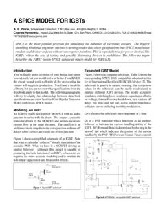
4 If any of these limits are exceeded, device functionality should not be assumed,damage may occur and reliability may be operation above the stresses listed in the Recommended Operating Ranges is not implied. Extended exposure to stresses beyond the RecommendedOperating Ranges limits mayaffect device parametric performance is indicated in the Electrical Characteristics for the listed test conditions, unless otherwise noted. Product performance may not beindicated by the Electrical Characteristics if operated under different / SIP8 LA3161 2 Package Dimensions unit : mm Block Diagram AMP1 AMP2NF1NF2 INPUT2 INPUT145 RequlatedVoltage CircuitOUTPUT1 OUTPUT2361287 GNDVCC SIP8 / SIP8 CASE 127 AGISSUE OLA3161 3 Test Circuit1 : VO, VG, THD, ICC, ri Test Circuit2 : VGO Test Circuit3 : Noise Sample Application Circuit 1.
5 Preamplifier for Car Stereo C547 FR2100k VCC = +18423675+CH1 ININCH210V1000pFC11000pFC3+ +10V+10V+R1R4100k +16 VLA3161C6C10150 C210 FC410 FC910 F100k R5R7100k C1147 C710 FC847 F VCCGNDOUTOUT++ LA3161 +R7R2++++C11000pFC31 000pFINGNDIN87 6 5 43 21C910 F10VC710 F10VC847 F 16VR4100k R5100k R1150 FC10C1147 F10VC410 F10V100k 100k LA3161 4 Function of External Parts C2, C4 are input coupling capacitors. In NAB equalizer amplifier, the gain at low frequencies is high and 1/f noise inside the IC is emphasized as output noise. Therefore, if the reactance of capacitor at low frequencies is increased, the dependence of 1/f noise on the signal source resistance causes the output noise voltage to deteriorate, and the value of reactance must be made small enough as compared with the signal source resistance.
6 C2, C4 also influence the operation start time and the adequate value of these capacitors is 10 F. (Since C2, C4 of less than F make the operation start time longer, use C2, C4, of F or more). C5, C11 are NF capacitors. The lower cut-off frequency depends on the value of these capacitors. If the lower cut-off frequency is taken as fL : C5 (C11) = 1/2 fL R2 (R7) If the value of this capacitor is made larger, the operation start time of amplifier is more delayed. The adequate value of capacitor is 47 F. The frequency characteristic of the equalizer amplifier depends on C6 and R4, R3 (C10 and R5, R6).
7 The time constants to obtain the standard NAB characteristic are as shown below. Tape C6 (R3 R4) 3180 s 1590 s R3 C6 90 s 120 s C8 is bias capacitor for the power line. C8 of 47 F is inserted at a point as close to the power supply pin (pin 4) as possible. C1, C3 are for preventing radio interference in the strong electric field, interference attributable to engine noise, and blocking oscillation at the time of large amplitude operation. The adequate value of C1, C3 is approximately 1000pF.
8 C7, C9 are output coupling capacitors. The adequate value of C7, C9 is 10 F. NAB element and determination of gain Since the DC feedback is provided by R1, R2 of NAB element, which brings about DC output potential at pins 3, 6, it is impossible to change the value of R1, R2 of NAB element greatly. Therefore, when determining the gain, change RNF with R1, R2, C1 (NAB element) kept constant. (1) How to obtain RNF Impedance Z of NAB element is Z = 11/R1 + j C1 + R2 = (R1 + R2) 1 + j C1{R1 R2/(R1 + R2)}1 + j C1R1 For a general negative feedback amplifier circuit, A = Ao/ (1 + Ao ) applies, and Z = A RNF is obtained under conditions of Ao>>A, A>>1 ( = RNF/ (RNF + Z), Ao = open-loop gain, A = feedback gain).
9 Therefore, we can use an approximation of RNF = Z/A. A = (VG for 1kHz) times, (Set R1, R2 at approximately 100k ) Each time constant of NAB characteristic. Tape T1 C1, R1 3180 s 1590 s T2 C1 (R1//R2) 90 s 120 s (2) Examples of NAB Constants (a) Tape speed : (8 tracks) VG : RNF (VG/f = 1kHz) VG 30 35 40 dB RNF 180 100 56 LA3161 5 (b) Tape speed : (cassette) VG.
10 RNF VG 30 35 40 dB RNF 440 240 130 (c) Flat amplifier VG : RNF VG 30 35 40 dB RNF 1 k Proper cares in using IC 1. Maximum Rating If the IC is used in the vicinity of the maximum rating, even a slight variation in conditions may cause the maximum rating to be exceeded, thereby leading to a breakdown. Allow an ample margin of variation for supply voltage, etc.