Example: bankruptcy
LPC81xM - NXP
Micro Trace Buffer (MTB) supported. Memory: Up to 16 kB on-chip flash programming me mory with 64 Byte page write and erase. Up to 4 kB SRAM. ROM API support: Boot loader. USART drivers. I2C drivers. Power profiles. Flash In-Application Programming (IAP) and In-System Programming (ISP). Digital peripherals:
Tags:
Information
Domain:
Source:
Link to this page:
Documents from same domain

P82B96 Dual bidirectional bus buffer - nxp.com
www.nxp.com1. General description The P82B96 is a bipolar IC that creates a non-latching, bidirectional, logic interface between the normal I2C-bus and a range of other bus configurations.It can interface

AN10441 Level shifting techniques in I2C-bus design
www.nxp.comDocument information AN10441 Level shifting techniques in I2C-bus design Rev. 01 — 18 June 2007 Application note Info Content Keywords I2C-bus, level shifting Abstract Logic level shifting may be required when interfacing legacy devices with

AN3234: Washing Machine Three-Phase AC …
www.nxp.comWashing Machine Three-Phase AC Induction Motor Drive, Rev. 0 Indirect Vector Control 4 Freescale Semiconductor If you are looking for more theory on the field ...

1. General description - nxp.com
www.nxp.com1. General description The TJA1044 is part of the Mantis family of high-speed CAN transceivers. It provides an interface between a Controller Area Network (CAN) protocol controller and the physical

PCA9570 Remote 4-bit general purpose outputs for 1 MHz …
www.nxp.com1. General description The PCA9570 is a CMOS device that provides 4 bits of General Purpose parallel Output (GPO) expansion in low voltage processor and handheld battery powered mobile

S32K144 EVB Quick Start Guide - NXP Semiconductors
www.nxp.comJ14 SWD connector. 3 EXTERNAL USE S32K144 EVBFeatures: ... USB connector of the USB cable to micro-B port J7 on the S32K144EVB. ... Windows, Linux and Mac operating systems. Using the MSD Flash Programmer 1. Locate the .srec file of your project , file is under the

Three-Phase BLDC Motor Sensorless Control Using …
www.nxp.comThis document describes the design of a three-phase brushless DC motor (BLDC motor) drive based on Freescale’s MC56F8013 and MC56F8023 dedicated motor control device. Brushless DC motors are popular in a wide application area.

AN11443 BFU550XR ISM 433 MHz LNA design - nxp.com
www.nxp.comAN11443 BFU550XR ISM 433 MHz LNA design Rev. 1 — 23 January 2014 Application note . Document information Info Content Keywords BFU520, BFU530, BFU550 series, ISM-band, 433MHz 866MHz Abstract This document describes an ISM Frequency LNA design on BFU5xxXR Starter kit

DSP56156 16-Bit Digital Signal Processor - nxp.com
www.nxp.comThe DSP56156 is a general-purpose MPU-style Digital Signal Processor (DSP). On a single semi- conductor chip, the DSP56156 comprises a very efficient 16-bit digital signal processing core, pro-

SAA7706H Car radio Digital Signal Processor (DSP)
www.nxp.comCar radio Digital Signal Processor (DSP) SAA7706H This text is here in white to force landscape pages to be rotated correctly when browsing through the pdf in the Acrobat reader.This text is here in _white to force landscape pages to be rotated correctly when browsing through the pdf in the Acrobat reader.This text is here inThis text is here in
Related documents
SN74LVC125A Quadruple Bus Buffer Gate With 3-State …
www.ti.comSN74LVC125A Quadruple Bus Buffer Gate With 3-State Outputs 1 Features 3 Description This quadruple bus buffer gate is designed for 1.65-V 1• 3-State Outputs to 3.6-V VCC operation. • Separate OE for all 4 buffers • Operates From 1.65 V to 3.6 V The SN74LVC125A device features independent line drivers with 3-state outputs. Each output is ...
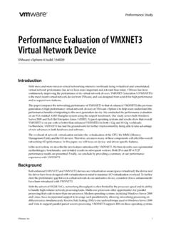
Performance Evaluation of VMXNET3 Virtual Network Device
www.vmware.comthe driver have been designed with virtualization in mind to minimize I/O virtualization overhead. To further ... VMXNET3 supports larger Tx/Rx ring buffer sizes compared to previous generations of virtual network devices. ... single session will be able to reach line rate for both transmit and receive. Overall, VMXNET3 throughput is ...

ARINC 429 Bus Interface - Actel
www.actel.comto buffer received data. Core429 supports multiple (configurable) ARINC 429 transmit channels and each channel can transmit data independently. Default Mode This is the recommended mode and allows the user to configure the core with user-defined transmit and ... Line Driver CPU

NVIDIA NVS 510 | NVIDIA NVS 510 Datasheet
www.nvidia.comFrame Buffer Memory 2 GB DDR3 Memory Interface 128-bit Memory Bandwidth 28.5 GB/s Max Power Consumption ... > Scriptable using WMI Command Line interface for integration with system-level management tools ... Unified Driver Architecture > Supports NVS …

Understanding the I2C Bus - Texas Instruments
www.ti.comlines, consisting of a buffer to read input data, and a pull-down FET to transmit data. A device is only able to pull the bus line low (provide short to ground) or release the bus line (high impedance to ground) and allow the pull-up resistor to raise the voltage. This is an important concept to realize when dealing with I2C

PCA9511A Hot swappable I2C-bus and SMBus bus buffer
www.nxp.comPCA9511A, the rise time accelerator’s circuits are turned on and the pull-down driver is turned off. 8.3 Maximum number of devices in series Each buffer adds about 0.1 V dynamic level offset at 25 °C with the offset larger at higher temperatures. Maximum offset (Voffset) is 0.150 V with a 10 kΩ pull-up resistor. The LOW

Introduction • SPI Pin Functionality Features
ww1.microchip.comUnidirectional SPI devices require just the clock line and one of the data lines. The device can use MISO line or the MOSI line depending on its purpose. 1.4. SPI Timing The SPI has four modes of operation, 0 through 3. These modes essentially control the way data is clocked in or out of an SPI device.
Creo® Parametric TOOLKIT User’s Guide - PTC
support.ptc.comInteractive Collection..... 484 Accessing Collection object from Selection Buffer ..... 487

Introduction to the Controller Area Network (CAN)
www.rpi.educontroller to move a correctly received frame to its proper position in a message buffer area. 3.1.2 Extended CAN S O F 11-Bit Identifier S R R I D E 18-Bit Identifier R T R r1 r0 DLC 0. . .8 Bytes Data CRC ACK E O F I F S Figure 3. Extended CAN: 29-Bit Identifier As shown in Figure 3, the Extended CAN message is the same as the Standard ...
Virtual GPU Software - NVIDIA Developer
docs.nvidia.comVirtual GPU Software DU-06920-001 _v14.0 Revision 02 | iii 2.5.1.4. Verifying the Installation of the NVIDIA vGPU Software for Citrix Hypervisor