Transcription of LTC3639 – High Efficiency, 150V 100mA Synchronous Step ...
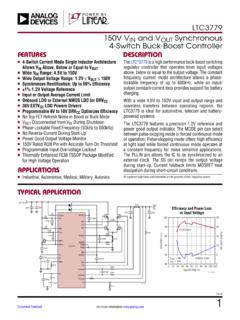
1 LTC363913639fcFor more information APPLICATION FEATURESDESCRIPTIONHigh Efficiency, 150V 100mA Synchronous Step-Down RegulatorThe LT C 3639 is a high efficiency step-down DC/DC regulator with internal high side and Synchronous power switches that draws only 12 A typical DC supply current while maintaining a regulated output voltage at no load. The LTC3639 can supply up to 100mA load current and features a programmable peak current limit that provides a simple method for optimizing efficiency and for reduc-ing output ripple and component size. The LTC3639 s combination of Burst Mode operation, integrated power switches, low quiescent current, and programmable peak current limit provides high efficiency over a broad range of load its wide input range of 4V to 150V and programmable overvoltage lockout, the LTC3639 is a robust regulator suited for regulating from a wide variety of power sources.
2 Additionally, the LTC3639 includes a precise run threshold and soft-start feature to guarantee that the power system start-up is well-controlled in any LTC3639 is available in a thermally enhanced high voltage-capable 16-lead MSE package with four missing , LT , LT C, LT M, Burst Mode, Linear Technology and the Linear logo are registered trademarks of Linear Technology Corporation. All other trademarks are the property of their respective and Power Loss vs Load Current5V to 150V Input to 5V Output, 100mA Step-Down RegulatorAPPLICATIONSn Wide Operating Input Voltage Range: 4V to 150Vn Synchronous Operation for Highest Efficiencyn Internal High Side and Low Side Power MOSFETsn No Compensation Requiredn Adjustable 10mA to 100mA Maximum Output Currentn Low Dropout Operation: 100% Duty Cyclen Low Quiescent Current: 12 A n Wide Output Range.
3 To VINn 1% Feedback Voltage Referencen Precise RUN Pin Thresholdn Internal or External Soft-Startn Programmable , , 5V or Adjustable Outputn Few External Components Required n Programmable Input Overvoltage Lockout n Thermally Enhanced High Voltage MSOP Packagen Industrial Control Suppliesn Medical Devicesn Distributed Power Systemsn Portable Instrumentsn Battery-Operated Devicesn Automotiven AvionicsSWVIN5V TO 150 VLTC3639470 H10 F3639 TA01a1 F200 VVOUT5V100mAGNDVFBSSVPRG1 RUNOVLOVPRG2 VINVIN = 12 VVIN = 36 VVIN = 72 VVIN = 150 VLOAD CURRENT (mA)30 EFFICIENCY (%)POWER LOSS (mW) TA01b01 EFFICIENCYPOWER LOSSVOUT = 5 VLTC363923639fcFor more information MAXIMUM RATINGS135678 SWVINFBOVPRG2 VPRG1 GND16141211109 GNDRUNOVLOISETSSVFBTOP VIEW17 GNDMSE PACKAGEVARIATION.
4 MSE16 (12)16-LEAD PLASTIC MSOP TJMAX = 150 C, JA = 40 C/W, JC = 10 C/W EXPOSED PAD (PIN 17) IS GND, MUST BE SOLDERED TO PCBPIN CONFIGURATIONORDER INFORMATIONLEAD FREE FINISHTAPE AND REELPART MARKING*PACKAGE DESCRIPTIONTEMPERATURE RANGELTC3639 EMSE#PBFLTC3639 EMSE#TRPBF363916-Lead Plastic MSOP 40 C to 125 CLTC3639 IMSE#PBFLTC3639 IMSE#TRPBF363916-Lead Plastic MSOP 40 C to 125 CLTC3639 HMSE#PBFLTC3639 HMSE#TRPBF363916-Lead Plastic MSOP 40 C to 150 CLTC3639 MPMSE#PBFLTC3639 MPMSE#TRPBF363916-Lead Plastic MSOP 55 C to 150 CConsult LT C Marketing for parts specified with wider operating temperature ranges. *The temperature grade is identified by a label on the shipping LT C Marketing for information on non-standard lead based finish more information on lead free part marking, go to: For more information on tape and reel specifications, go to: Supply Voltage.
5 To 150 VRUN to 150 VSS, FBO, OVLO, ISET Voltages .. to 6 VVFB, VPRG1, VPRG2 Voltages .. to 6 VOperating Junction Temper atur e Range (Notes 2, 3) LTC3639E, LTC3639I .. 40 C to 125 C LTC3639H .. 40 C to 150 C LTC3639MP .. 55 C to 150 CStorage Temper atur e Range .. 65 C to 150 CLead Temper atur e (Soldering, 10 sec) ..300 C(Note 1)ELECTRICAL CHARACTERISTICS The l denotes the specifications which apply over the specified operating junction temperature range, otherwise specifications are at TA = 25 C (Note 2). VIN = 12V, unless otherwise Supply (VIN)VINI nput Voltage Operating Range4150 VVOUTO utput Voltage Operating Undervoltage LockoutVIN Rising VIN Falling Hysteresisl V mVIQDC Supply Current (Note 4) Active Mode Sleep Mode Shutdown Mode No Load VRUN = 0V 150 12 350 22 6 A A AVRUNRUN Pin ThresholdRUN Rising RUN Falling V mVIRUNRUN Pin Leakage CurrentRUN = 10010nAVOVLOOVLO Pin ThresholdOVLO Rising OVLO Falling V mVLTC363933639fcFor more information CHARACTERISTICS The l denotes the specifications which apply over the specified operating junction temperature range, otherwise specifications are at TA = 25 C (Note 2).
6 VIN = 12V, unless otherwise Supply (VFB)VFB(ADJ)Feedback Comparator Threshold (Adjustable Output)VFB Rising, VPRG1 = VPRG2 = 0V LT C3639E, LT C3639I LTC 3639H, LT C3639MP l l V VVFBHF eedback Comparator Hysteresis (Adjustable Output)VFB Falling, VPRG1 = VPRG2 = 0Vl359mVIFBF eedback Pin CurrentVFB = 1V, VPRG1 = VPRG2 = 0V 10010nAVFB(FIXED)Feedback Comparator Thresholds (Fixed Output)VFB Rising, VPRG1 = SS, VPRG2 = 0V VFB Falling, VPRG1 = SS, VPRG2 = 0Vl VVFB Rising, VPRG1 = 0V, VPRG2 = SS VFB Falling, VPRG1 = 0V, VPRG2 = SSl VVFB Rising, VPRG1 = VPRG2 = SS VFB Falling, VPRG1 = VPRG2 = SSl VOperationIPEAKPeak Current Comparator ThresholdISET Floating 100k Resistor from ISET to GND ISET Shorted to GNDl l l200 100 17230 120 25260 140 30mA mA mARONP ower Switch On-Resistance Top Switch Bottom Switch ISW = 50mA ISW = 50mA ILSWS witch Pin Leakage CurrentVIN = 150V, SW = AISSSoft-Start Pin Pull-Up CurrentVSS < AtINT(SS)Internal Soft-Start TimeSS Pin Floating1msNote 1.
7 Stresses beyond those listed under Absolute Maximum Ratings may cause permanent damage to the device. Exposure to any Absolute Maximum Rating condition for extended periods may affect device reliability and 2: The LTC3639 is tested under pulsed load conditions such that TJ TA. The LTC3639E is guaranteed to meet performance specifications from 0 C to 85 C. Specifications over the 40 C to 125 C operating junction temperature range are assured by design, characterization and correlation with statistical process controls. The LTC3639I is guaranteed over the 40 C to 125 C operating junction temperature range, the LTC3639H is guaranteed over the 40 C to 150 C operating junction temperature range and the LTC3639MP is tested and guaranteed over the 55 C to 150 C operating junction temperature range.
8 High junction temperatures degrade operating lifetimes; operating lifetime is derated for junction temperatures greater than 125 C. Note that the maximum ambient temperature consistent with these specifications is determined by specific operating conditions in conjunction with board layout, the rated package thermal impedance and other environmental factors. Note 3: The junction temperature (TJ, in C) is calculated from the ambient temperature (TA, in C) and power dissipation (PD, in Watts) according to the formula: TJ = TA + (PD JA)where JA is 40 C/W for the MSOP that the maximum ambient temperature consistent with these specifications is determined by specific operating conditions in conjunction with board layout, the rated package thermal impedance and other environmental factors.
9 Note 4: Dynamic supply current is higher due to the gate charge being delivered at the switching frequency. See Applications more information PERFORMANCE CHARACTERISTICSPeak Current Trip Threshold vs RISETE fficiency vs Load Current, VOUT = 5 VPeak Current Trip Threshold vs TemperatureEfficiency vs Load Current, VOUT = Current Trip Threshold vs Input VoltageEfficiency vs Load Current, VOUT = vs Input Voltage, VOUT = 5 VFeedback Comparator Trip Threshold vs TemperatureRUN and OVLO Comparator Threshold vs TemperatureLOAD CURRENT (mA)30 EFFICIENCY (%) G0101 ISET OPENFIGURE 13 CIRCUITVIN = 12 VVIN = 36 VVIN = 72 VVIN = 150V309010020108050706040002575100501251 50 VIN VOLTAGE (V)EFFICIENCY (%)3639 G04 ILOAD = 100mAILOAD = 10mAILOAD = 1mAISET OPENFIGURE 13 CIRCUITTEMPERATURE ( C)
10 55798 THRESHOLD VOLTAGE (V)799800801802 25535653639 G0595125155 RISET (k )01502002501753639 G0710050501007525125 1502000 PEAK CURRENT TRIP THRESHOLD (mA)TEMPERATURE ( C) 55 PEAK CURRENT (mA)1002001553639 G08500565 253595125150250300 ISET OPENISET = GNDRISET = 100k VIN VOLTAGE (V)0 PEAK CURRENT (mA)1002001503639 G09500603090120150250300 ISET OPENISET = GNDRISET = 100k TEMPERATURE ( C) 55 RUN OR OVLO THRESHOLD VOLTAGE (V) CURRENT (mA)30 EFFICIENCY (%) G0201 ISET OPENFIGURE 13 CIRCUITVIN = 12 VVIN = 36 VVIN = 72 VVIN = 150 VLOAD CURRENT (mA)30 EFFICIENCY (%) G0301 ISET OPENFIGURE 13 CIRCUITVIN = 12 VVIN = 36 VVIN = 72 VVIN = 150 VLTC363953639fcFor more information PERFORMANCE CHARACTERISTICSS witch On-Resistance vs Input VoltageSwitch On-Resistance vs TemperatureLoad Step Transient ResponseQuiescent Supply Current vs Input VoltageOperating Waveforms, VIN = 48 VQuiescent Supply Current vs TemperatureOperating Waveforms, VIN = 150 VSwitch Leakage Current vs TemperatureShort-Circuit and RecoveryVIN VOLTAGE (V)00 VIN SUPPLY CURRENT ( A)1560903639 G1010530120150 SLEEPSHUTDOWNVIN VOLTAGE (V)1 SWITCH ON-RESISTANCE ( )274 TOP3639 G135630609030120150 BOTTOMTEMPERATURE ( C) 55 SWITCH ON-RESISTANCE ( )