Transcription of Negative Voltage Regulators - ON Semiconductor
1 Semiconductor Components Industries, LLC, 1994 April, 2021 Rev. 111 Publication Order Number:MC79L00/DNegative Voltage Regulators100 mAMC79L00A SeriesThe MC79L00A Series Negative Voltage Regulators areinexpensive, easy to use devices suitable for numerous applicationsrequiring up to 100 mA. Like the higher powered MC7900 Seriesnegative Regulators , this series features thermal shutdown and currentlimiting, making them remarkably rugged. In most applications, noexternal components are required for MC79L00A devices are useful for on card regulation or anyother application where a regulated Negative Voltage at a modestcurrent level is needed. These Regulators offer substantial advantageover the common resistor/Zener diode No External Components Required Internal Short Circuit Current Limiting Internal Thermal Overload Protection Low Cost Complementary Positive Regulators Offered (MC78L00 Series) Pb Free Packages are Available* Automotive temperature range selections are available with special test conditionsand additional tests in 5, 12 and 15 V devices.
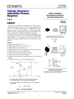
2 Contact your local ON Semiconductorsales office for 1. Representative Schematic DiagramTHREE TERMINAL LOWCURRENT Negative FIXEDVOLTAGE REGULATORSTO 92P SUFFIXCASE 29 10 SOIC 8D SUFFIXCASE 751 MARKINGDIAGRAMSSee detailed ordering and shipping information in the packagedimensions section on page 7 of this data INFORMATIONPin 1. Ground2. Input3. OutputPin 1. Vout2. Vin3. Vin4. NC5. GND6. Vin7. Vin8. NCxxx= Specific Device CodeA= Assembly LocationL= Wafer LotY= YearW= Work Weeky= B or LEADSTRAIGHT LEAD3MC79L00A RATINGS (TA = +25 C, unless otherwise noted.)RatingSymbolValueUnitInput Voltage ( 5 V)( 12, 15, 18 V)( 24 V)VI 30 35 40 VdcPower DissipationCase 29 (TO 92 Type)TA = 25 CThermal Resistance, Junction to AmbientThermal Resistance, Junction to CaseCase 751 (SOIC 8 Type) (Note 1)TA = 25 CThermal Resistance, Junction to AmbientThermal Resistance, Junction to CasePDRqJARqJCPDRqJARqJCInternally Limited16083 Internally Limited18045W C/W C/WW C/W C/WStorage Temperature RangeTstg 65 to +150 CJunction TemperatureTJ+150 CStresses exceeding those listed in the Maximum Ratings table may damage the device.
3 If any of these limits are exceeded, device functionalityshould not be assumed, damage may occur and reliability may be SOIC 8 Junction to Ambient Thermal Resistance is for minimum recommended pad size. Refer to Figure 9 for Thermal Resistance variationversus pad size.*This device series contains ESD protection and exceeds the following tests:Human Body Model 2000 V per MIL_STD_883, Method 3015 Machine Model Method 200 CHARACTERISTICS (VI = 10 V, IO = 40 mA, CI = mF, CO = mF, 40 C < TJ +125 C (for MC79 LXXAB),0 C < TJ < +125 C (for MC79 LXXAC)).MC79L05AC, ABCharacteristicsSymbolMinTypMaxUnitOutp ut Voltage (TJ = +25 C)VO Regulation (TJ = +25 C) Vdc VI 20 Vdc Vdc VI 20 VdcRegline 150100mVLoad RegulationTJ = +25 C, mA IO 100 mA IO 40 mARegload 6030mVOutput Voltage Vdc VI 20 Vdc, mA IO 40 mAVI = 10 Vdc, mA IO 70 mAVO Bias Current(TJ = +25 C)(TJ = +125 C)IIB Bias Current Change Vdc VI 20 mA IO 40 mAIIB noise Voltage (TA = +25 C, 10 Hz f 100 kHz)Vn 40 mVRipple Rejection ( VI 18 Vdc, f = 120 Hz, TJ = +25 C)RR4149 dBDropout Voltage (IO = 40 mA, TJ = +25 C)
4 |VI VO| VdcProduct parametric performance is indicated in the Electrical Characteristics for the listed test conditions, unless otherwise noted. Productperformance may not be indicated by the Electrical Characteristics if operated under different CHARACTERISTICS (VI = 19 V, IO = 40 mA, CI = mF, CO = mF, 40 C < TJ +125 C (for MC79 LXXAB),0 C < TJ < +125 C (for MC79 LXXAC)).MC79L12AC, ABCharacteristicsSymbolMinTypMaxUnitOutp ut Voltage (TJ = +25 C)VO 12 Regulation (TJ = +25 C) Vdc VI 27 Vdc 16 Vdc VI 27 VdcRegline 250200mVLoad RegulationTJ = +25 C, mA IO 100 mA IO 40 mARegload 10050mVOutput Voltage Vdc VI 27 Vdc, mA IO 40 mAVI = 19 Vdc, mA IO 70 mAVO Bias Current(TJ = +25 C)(TJ = +125 C)IIB Bias Current Change 16 Vdc VI 27 mA IO 40 mAIIB noise Voltage (TA = +25 C, 10 Hz f 100 kHz)Vn 80 mVRipple Rejection ( 15 VI 25 Vdc, f = 120 Hz, TJ = +25 C)RR3742 dBDropout Voltage (IO = 40 mA, TJ = +25 C)
5 |VI VO| VdcProduct parametric performance is indicated in the Electrical Characteristics for the listed test conditions, unless otherwise noted. Productperformance may not be indicated by the Electrical Characteristics if operated under different CHARACTERISTICS (VI = 23 V, IO = 40 mA, CI = mF, CO = mF, 40 C < TJ +125 C (for MC79 LXXAB),0 C < TJ < +125 C (for MC79 LXXAC)).MC79L15AC, ABCharacteristicsSymbolMinTypMaxUnitOutp ut Voltage (TJ = +25 C)VO 15 Regulation (TJ = +25 C) Vdc VI 30 Vdc 20 Vdc VI 30 VdcRegline 300250mVLoad RegulationTJ = +25 C, mA IO 100 mA IO 40 mARegload 15075mVOutput Voltage Vdc VI Vdc, mA IO 40 mAVI = 23 Vdc, mA IO 70 mAVO Bias Current(TJ = +25 C)(TJ = +125 C)IIB Bias Current Change 20 Vdc VI 30 mA IO 40 mADIIB noise Voltage (TA = +25 C, 10 Hz f 100 kHz)VN 90 mVRipple Rejection ( VI Vdc, f = 120 Hz)
6 RR3439 dBDropout Voltage IO = 40 mA, TJ = +25 C|VI VO| VdcProduct parametric performance is indicated in the Electrical Characteristics for the listed test conditions, unless otherwise noted. Productperformance may not be indicated by the Electrical Characteristics if operated under different CHARACTERISTICS (VI = 27 V, IO = 40 mA, CI = mF, CO = mF, 40 C < TJ +125 C (for MC79 LXXAB),0 C < TJ < +125 C (for MC79 LXXAC), unless otherwise noted).MC79L18 ACCharacteristicsSymbolMinTypMaxUnitOutp ut Voltage (TJ = +25 C)VO 18 Regulation (TJ = +25 C) Vdc VI 33 Vdc Vdc VI 33 Vdc 22 Vdc VI 33 Vdc 21 Vdc VI 33 VdcRegline 325 275mVLoad RegulationTJ = +25 C, mA IO 100 mA IO 40 mARegload 17085mVOutput Voltage Vdc VI 33 Vdc, mA IO 40 mA Vdc VI 33 Vdc, mA IO 40 mAVI = 27 Vdc, mA IO 70 mAVO Bias Current(TJ = +25 C)(TJ = +125 C)IIB Bias Current Change 21 Vdc VI 33 Vdc 27 Vdc VI 33 mA IO 40 mAIIB noise Voltage (TA = +25 C, 10 Hz f 100 kHz)Vn 150 mVRipple Rejection ( 23 VI 33 Vdc, f = 120 Hz, TJ = +25 C)
7 RR3348 dBDropout Voltage IO = 40 mA, TJ = +25 C|VI VO| VdcProduct parametric performance is indicated in the Electrical Characteristics for the listed test conditions, unless otherwise noted. Productperformance may not be indicated by the Electrical Characteristics if operated under different CHARACTERISTICS (VI = 33 V, IO = 40 mA, CI = mF, CO = mF, 40 C < TJ +125 C (for MC79 LXXAB),0 C < TJ < +125 C (for MC79 LXXAC), unless otherwise noted).MC79L24 ACCharacteristicsSymbolMinTypMaxUnitOutp ut Voltage (TJ = +25 C)VO 23 24 25 VdcInput Regulation (TJ = +25 C) 27 Vdc VI 38 Vdc Vdc VI 38 Vdc 28 Vdc VI 38 VdcRegline 350 300mVLoad RegulationTJ = +25 C, mA IO 100 mA IO 40 mARegload 200100mVOutput Voltage 27 Vdc VI 38 V, mA IO 40 mA 28 Vdc VI 38 Vdc, mA IO 40 mAVI = 33 Vdc, mA IO 70 mAVO Bias Current(TJ = +25 C)(TJ = +125 C)IIB Bias Current Change 28 Vdc VI 38 mA IO 40 mADIIB noise Voltage (TA = +25 C, 10 Hz f 100 kHz)Vn 200 mVRipple Rejection ( 29 VI 35 Vdc, f = 120 Hz, TJ = +25 C)
8 RR3147 dBDropout Voltage IO = 40 mA, TJ = +25 C|VI VO| VdcProduct parametric performance is indicated in the Electrical Characteristics for the listed test conditions, unless otherwise noted. Productperformance may not be indicated by the Electrical Characteristics if operated under different INFORMATIOND esign ConsiderationsThe MC79L00A Series of fixed Voltage Regulators aredesigned with Thermal Overload Protections that shutsdown the circuit when subjected to an excessive poweroverload condition, Internal Short Circuit Protection thatlimits the maximum current the circuit will many low current applications, compensationcapacitors are not required. However, it is recommendedthat the regulator input be bypassed with a capacitor if theregulator is connected to the power supply filter with longwire length, or if the output load capacitance is large.
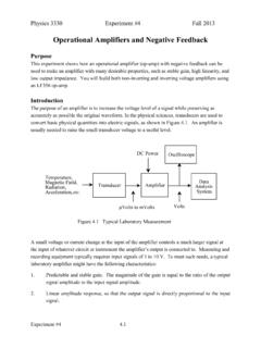
9 Aninput bypass capacitor should be selected to provide goodhigh frequency characteristics to insure stable operationunder all load conditions. A mF or larger tantalum,mylar, or other capacitor having low internal impedance athigh frequencies should be chosen. The bypass capacitorshould be mounted with the shortest possible leads directlyacross the regulator s input terminals. Normally goodconstruction techniques should be used to minimize groundloops and lead resistance drops since the regulator has noexternal sense lead. Bypassing the output is 2. Positive and Negative RegulatorFigure 3. Standard Application+Vin+ ** * common ground is required between the input and the outputvoltages.
10 The input Voltage must remain typically V abovethe output Voltage even during the low point on the ripple Voltage . * CI is required if regulator is located an appreciable * distance from the power supply filter** CO improves stability and transient CHARACTERISTICS(TA = +25 C, unless otherwise noted.)IIB, INPUT BIAS CURRENT (mA)IIB, INPUT BIAS CURRENT (mA)VO, OUTPUT Voltage (V)Figure 4. Dropout CharacteristicsFigure 5. Dropout Voltage versusJunction TemperatureFigure 6. Input Bias Current versusAmbient TemperatureFigure 7. Input Bias Current versusInput VoltageFigure 8. Maximum Average Power Dissipationversus Ambient Temperature (TO 92) , INPUT Voltage (V)MC79L05C VO = VTJ = 25 CIO = mAIO = 100 mAIO = 40 , INPUT/OUTPUT DIFFERENTIALVOLTAGE (V)IOTJ, JUNCTION TEMPERATURE ( C)IO = 70 , AMBIENT TEMPERATURE ( C)MC79L05C Vin = -10 VVO = VIO = 40 , INPUT Voltage (V)MC79L05C VO = VIO = 40 mA10,0001,00010010, POWER DISSIPATION (mW)DTA, AMBIENT TEMPERATURE ( C)255075100125150 PNo HeatsinkRqJA = 200 C/WPD(max) to 25 C = 625 mWFigure 9.