Transcription of Overvoltage, Undervoltage and Reverse Supply Protection ...
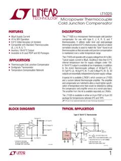
1 LTC43651 Rev. BFor more information FeedbackTYPICAL APPLICATION FEATURESDESCRIPTION Overvoltage, Undervoltage and Reverse Supply Protection Controller12V Automotive ApplicationAPPLICATIONSn Wide Operating voltage Range: to 34Vn Overvoltage Protection to 60Vn Reverse Supply Protection to 40Vn LTC4365: Blocks 50Hz and 60Hz AC Powern LTC4365-1: Fast (1ms) Recovery from Faultn No Input Capacitor or TVS Required for Most Applicationsn Adjustable Undervoltage and Overvoltage Protection Rangen Charge Pump Enhances External N-Channel MOSFETn Low Operating Current: 125 An Low Shutdown Current: 10 An Compact 8-Lead, 3mm 2mm DFN and TSOT-23 (ThinSOT ) Packages nAEC-Q100 Qualified for Automotive Applicationsn Portable Instrumentationn Industrial Automationn Laptopsn Automotive Surge ProtectionAll registered trademarks and trademarks are the property of their respective owners.
2 Protected by patents, including XXXXX, Protected from Reverse and Overvoltage at VINThe LT C 4365 protects applications where power Supply input voltages may be too high, too low or even negative. It does this by controlling the gate voltages of a pair of external N-channel MOSFETs to ensure that the output stays within a safe operating LTC4365 can withstand voltages between 40V and 60V and has an operating range of to 34V, while consuming only 125 A in normal o comparator inputs allow configuration of the over- voltage (OV) and Undervoltage (UV) set points using an external resistive divider. A shutdown pin provides external control for enabling and disabling the MOSFETs as well as placing the device in a low current shutdown state. A fault output provides status of the gate pin pulling low. A fault is indicated when the part is in shutdown or the input voltage is outside the UV and OV set LTC4365 has a 36ms turn-on delay that debounces live connections and blocks 50Hz to 60Hz AC power.
3 For fast recovery after faults, the LTC4365-1 has a reduced 1ms turn-on delay. 30 VGND10V/DIV30V4365 TA01b1s/DIVUV = 5 VOV = 18 VVOUTVOUTVINVINVALIDWINDOWVINUVOVSHDNOV = 18 VUV = 5V4365 BFor more information Free FinishTAPE AND REEL (MINI)TAPE AND REELPART MARKING*PACKAGE DESCRIPTIONTEMPERATURE RANGELTC4365 CDDB#TRMPBFLTC4365 CDDB#TRPBFLFKS8-Lead (3mm 2mm) Plastic DFN0 C to 70 CLTC4365 CDDB-1#TRMPBFLTC4365 CDDB-1#TRPBFLGMB8-Lead (3mm 2mm) Plastic DFN0 C to 70 CLTC4365 IDDB#TRMPBFLTC4365 IDDB#TRPBFLFKS8-Lead (3mm 2mm) Plastic DFN 40 C to 85 CLTC4365 IDDB-1#TRMPBFLTC4365 IDDB-1#TRPBFLGMB8-Lead (3mm 2mm) Plastic DFN 40 C to 85 CLTC4365 HDDB#TRMPBFLTC4365 HDDB#TRPBFLFKS8-Lead (3mm 2mm) Plastic DFN 40 C to 125 CLTC4365 HDDB-1#TRMPBFLTC4365 HDDB-1#TRPBFLGMB8-Lead (3mm 2mm) Plastic DFN 40 C to 125 CLTC4365 CTS8#TRMPBFLTC4365 CTS8#TRPBFLTFKT8-Lead Plastic TSOT-230 C to 70 CLTC4365 CTS8-1#TRMPBFLTC4365 CTS8-1#TRPBFLTGKZ8-Lead Plastic TSOT-230 C to 70 CLTC4365 ITS8#TRMPBFLTC4365 ITS8#TRPBFLTFKT8-Lead Plastic TSOT-23 40 C to 85 CLTC4365 ITS8-1#TRMPBFLTC4365 ITS8-1#TRPBFLTGKZ8-Lead Plastic TSOT-23 40 C to 85 CLTC4365 HTS8#TRMPBFLTC4365 HTS8#TRPBFLTFKT8-Lead Plastic TSOT-23 40 C to 125 CLTC4365 HTS8-1#TRMPBFLTC4365 HTS8-1#TRPBFLTGKZ8-Lead Plastic TSOT-23 40 C to 125 CPIN CONFIGURATIONABSOLUTE MAXIMUM RATINGSS upply voltage (Note 1) VIN.
4 40V to 60 VInput Voltages (Note 3) UV, SHDN .. to 60V OV .. to 6V to 40 VOutput Voltages (Note 4) FAULT .. to 60V GATE .. 40V to 45V TOP VIEW9 GNDDDB PACKAGE8-LEAD (3mm 2mm) PLASTIC DFN56784321 GNDOVUVVINSHDNFAULTVOUTGATE TJMAX = 150 C, JA = 76 C/W EXPOSED PAD (PIN 9) PCB GROUND CONNECTION OPTIONAL 12348765 TOP VIEWTS8 PACKAGE8-LEAD PLASTIC TSOT-23 GATEVOUTFAULTSHDNVINUVOVGND TJMAX = 150 C, JA = 195 C/WORDER INFORMATIONI nput Currents UV, OV, SHDN .. 1mAOperating Ambient Temper atur e Range LTC 4365C ..0 C to 70 C LTC 4365I .. 40 C to 85 C LTC 4365H .. 40 C to 125 CStorage Temper atur e Range .. 65 C to 150 CLead Temper atur e (Soldering, 10 sec) for TSOT Only ..300 CLTC43653 Rev. BFor more information Free FinishAUTOMOTIVE PRODUCTS**TAPE AND REEL (MINI)TAPE AND REELPART MARKING*PACKAGE DESCRIPTIONTEMPERATURE RANGELTC4365 ITS8#WTRMPBFLTC4365 ITS8#WTRPBFLTFKT8-Lead Plastic TSOT-23 40 C to 85 CLTC4365 ITS8-1#WTRMPBFLTC4365 ITS8-1#WTRPBFLTGKZ8-Lead Plastic TSOT-23 40 C to 85 CLTC4365 HTS8#WTRMPBFLTC4365 HTS8#WTRPBFLTFKT8-Lead Plastic TSOT-23 40 C to 125 CLTC4365 HTS8-1#WTRMPBFLTC4365 HTS8-1#WTRPBFLTGKZ8-Lead Plastic TSOT-23 40 C to 125 CContact the factory for parts specified with wider operating temperature ranges.
5 *The temperature grade is identified by a label on the shipping and reel specifications. Some packages are available in 500 unit reels through designated sales channels with #TRMPBF suffix.**Versions of this part are available with controlled manufacturing to support the quality and reliability requirements of automotive applications. These models are designated with a #W suffix. Only the automotive grade products shown are available for use in automotive applications. Contact your local Analog Devices account representative for specific product ordering information and to obtain the specific Automotive Reliability reports for these CHARACTERISTICSSYMBOLPARAMETERCONDITIONS MINTYPMAXUNITSVIN, VOUTVINI nput voltage RangeOperating Range Protection Rangel 40 34 60V VIVINI nput Supply CurrentSHDN = 0V, VIN = VOUT, 40 C to 85 C SHDN = 0V, VIN = VOUT, 40 C to 125 C SHDN = l l10 10 2550 100 150 A A AIVIN(R) Reverse Input Supply CurrentVIN = 40V, VOUT = 0Vl (UVLO)Input Supply Undervoltage LockoutVIN Input CurrentSHDN = 0V, VIN = VOUT SHDN = , VIN = VOUT VIN = 40V, VOUT = 0Vl l l6 100 2030 250 50 A A AGATE VGATEN-Channel Gate Drive (GATE-VOUT)VIN = VOUT = , IGATE = 1 A VIN = VOUT = 12V to 34V, IGATE = 1 Al l3 VIGATE(UP)N-Channel Gate Pull Up CurrentGATE = VIN = VOUT = 12Vl 12 20 30 AIGATE(FAST)
6 N- Channel Gate Fast Pull Down CurrentFast Shutdown, GATE = 20V, VIN = VOUT = 12Vl315072mAIGATE(SLOW)N-Channel Gate Gentle Pull Down CurrentGentle Shutdown, GATE = 20V, VIN = VOUT = 12Vl5090150 AtGATE(FAST)N-Channel Gate Fast Turn Off DelayCGATE = , UV or OV Faultl24 stGATE(SLOW)N-Channel Gentle Turn Off DelayCGATE = , SHDN Falling, VIN = VOUT = 12Vl150250350 stRECOVERYGATE Recovery Delay TimeVIN = 12V, Power Good to VGATE > 0V LTC4365, CGATE = LTC4365-1, CGATE = l l 26 36 1 49 ms ms The l denotes the specifications which apply over the full operating temperature range, otherwise specifications are at TA = 25 C. VIN = to 34V, unless otherwise noted. (Note 2)ORDER INFORMATIONLTC43654 Rev. BFor more information , OVVUVUV Input Threshold VoltageUV Falling VGATE = Input Threshold VoltageOV Rising VGATE = Input Hysteresisl202532mVVOVHYSTOV Input Hysteresisl202532mVILEAKUV, OV Leakage CurrentV = , VIN = 34Vl 10nAtFAULTUV, OV Fault Propagation DelayOverdrive = 50mV VIN = VOUT = 12Vl12 sSHDNVSHDNSHDN Input ThresholdSHDN Falling to VGATE = Input CurrentSHDN = , VIN = 34Vl 10nAtSTARTD elay Coming Out of Shutdown ModeSHDN Rising to VGATE > 0V, VIN = VOUT = 12Vl4008001200 stSHDN(F)SHDN to FAULT AssertedVIN = VOUT = stLOWPWRD elay from Turn Off to Low Power OperationVIN = VOUT = 12V LTC4365 LTC4365-1 l l 26 36 55 2 ms msFAULTVOLFAULT Output voltage LowIFAULT = 500 Leakage CurrentFAULT = 5V, VIN = 34Vl 20nANote 1.
7 Stresses beyond those listed under Absolute Maximum Ratings may cause permanent damage to the device. Exposure to any Absolute Maximum Rating condition for extended periods may affect device reliability and 2. All currents into pins are positive; all voltages are referenced to GND unless otherwise 3. These pins can be tied to voltages below through a resistor that limits the current below 4. The GATE pin is referenced to VOUT and does not exceed 44V for the entire operating CHARACTERISTICS The l denotes the specifications which apply over the full operating temperature range, otherwise specifications are at TA = 25 C. VIN = to 34V, unless otherwise noted. (Note 2)LTC43655 Rev. BFor more information PERFORMANCE CHARACTERISTICSVOUT Operating Current vs TemperatureVOUT Shutdown Current vs TemperatureVOUT Current vs Reverse VINVIN Operating Current vs TemperatureVIN Shutdown Current vs VINVIN Current vs VIN ( 40 to 60V)GATE Current vs GATE DriveGATE Drive vs VINGATE Drive vs TemperatureTEMPERATURE ( C) 500 IVIN ( A)204060800501004365 G01100 252575125 SHDN = = 12 VVIN = 34 VVOUT = VINVIN = (V)00 IVIN ( A)510152520102035304365 G023051525 VIN = VOUTSHDN = 0V25 C 45 C125 C70 CVIN (V) 50 1600 IVIN ( A) 1200 800 4000050754365 G03400 2525 SHDN = UV = 0V25 C25 C 45 C125 CTEMPERATURE ( C) 500 IVOUT ( A)40801201600100751254365 G04200 252550 SHDN = = 34 VVOUT = 12 VVOUT = = VOUTTEMPERATURE ( C) 500 IVOUT ( A)51015025751001254365 G0520 2550 SHDN = 0 VVOUT = 34 VVOUT = 12 VVOUT = = VOUTVIN (V)0 IVOUT ( A)
8 51015200 10 30 40 504365 G0625 20 45 C25 C125 CVOUT = 0 VVIN (V)0 VGATE (V)2468100515203525304365 G071210 VOUT = 0 VVOUT = VINT = 25 CIGATE = 1 ATEMPERATURE ( C) 500 VGATE (V)24680501004365 G0810 252575125 VIN = VOUT = 12 VVIN = VOUT = 34 VIGATE = 1 AVIN = VOUT = VGATE (V)00 IGATE(UP) ( A) 5 10 15 2026104365 G09 2548 VIN = VOUT = 12V125 C25 C 45 CLTC43656 Rev. BFor more information Propagation Delay vs OverdriveRecovery Delay Time vs TemperatureLTC4365 Recovery Delay Time vs VIN OV Threshold vs TemperatureUV/OV Leakage vs TemperatureUV Threshold vs TemperatureTYPICAL PERFORMANCE CHARACTERISTICSTEMPERATURE ( C) (mV) 252575125 VIN = VOUT = 12 VTEMPERATURE ( C) (mV) 252575125 VIN = VOUT = 12 VTEMPERATURE ( C) 750 ILEAK (nA) 252575175125 VUV/OV = VIN = 12 VUVOVOVERDRIVE (mV)10tFAULT ( s)8412164365 G1320101001000 VIN = VOUT = 12VT = 25 CTEMPERATURE ( C) 500tRECOVERY (ms)10203040500501004365 G14 252575125 VIN = 34 VVIN = 12 VVIN = (V)00tRECOVERY (ms)
9 10203040501020354365 G155153025125 C25 C 45 C4365 F, 1k LOAD ON VOUT60V DUAL NCH MOSFET1V/DIV20V/DIVGNDGND4365 G17250 s/DIVVOUTGATE100 F, 12 LOAD ON VOUT60V SI9945 DUAL NCH MOSFETVIN = 12 VSHDN5V/DIV3V/DIVGNDGND4365 G18250 s/DIVVOUTSHDNGATE100 F, 12 LOAD ON VOUT60V SI9945 DUAL NCH MOSFET5V/DIV3V/DIVGNDGNDLTC4365 AC BlockingTurn-On TimingTurn-Off TimingLTC43657 Rev. BFor more information FUNCTIONSE xposed Pad: Connect to device : Fault Indication Output. This high voltage open drain output is pulled low if UV is below its monitor threshold, if OV is above its monitor threshold, if SHDN is low, or if VIN has not risen above VIN(UVLO).GATE: Gate Drive Output for External N-channel MOSFETs. An internal charge pump provides 20 A of pull-up current and up to of enhancement to the gate of an external N-channel MOSFET. When turned off, GATE is pulled just below the lower of VIN or VOUT.
10 When VIN goes negative, GATE is automati-cally connected to : Device : Overvoltage Comparator Input. Connect this pin to an external resistive divider to set the desired VIN overvoltage fault threshold. The OV input connects to an accurate, fast (1 s) comparator with a rising threshold and 25mV of hysteresis. When OV rises above its threshold, a 50mA current sink pulls down on the GATE output. When OV falls back below , and after a 36ms recovery delay waiting period (1ms for LTC4365-1), the GATE charge pump is enabled. The low leakage current of the OV input allows the use of large valued resistors for the external resistive divider. Connect to GND if : Shutdown Control Input. SHDN high enables the GATE charge pump which in turn enhances the gate of an external N-channel MOSFET. A low on SHDN generates a pull down on the GATE output with a 90 A current sink and places the LTC4365 in low current mode (10 A).
