Transcription of Semiconductor Assembly Technologies for the …
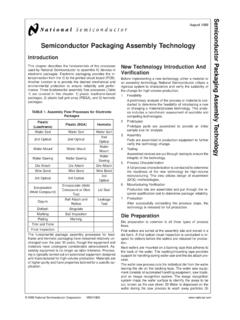
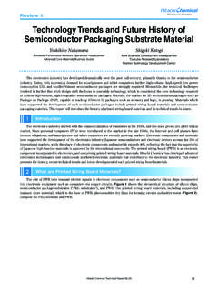
1 Hitachi Review Vol. 50 (2001), No. 2 55 Semiconductor Assembly Technologies for the Network EraOVERVIEW: The network era of the 21st century requires that both desktop-type equipment and mobile equipment be connected to networks for theexchange of data and information. Improvements to hardware, in the formof higher speeds of data transmission and information processing, will berequired. Furthermore, higher-density Assembly and lower levels of powerconsumption will be called for to realize lighter and more compact mobileequipment. Consequently, the Semiconductor Assembly technology for suchequipment will not be the conventional surface mounting technology .
2 Hitachihas been focusing on the development of a new Assembly technology tomeet these NishiMunehisa KishimotoKunio KobayashiTakashi AkazawaToshihiko SatoINTRODUCTIONIN the 21st century, remarkable changes are going tooccur with respect to the Semiconductor assemblytechnology used to produce equipment for networkapplications. Mobile equipment will be required to belighter and more compact, whereas servers and routerswill require faster processing and higher densities following explains Hitachi s semiconductorassembly technology that will be used to meet theseneeds, centering on the cellular phone, which isexpected to lead the way in high-density IN ELECTRONIC EQUIPMENT ANDTHE NEED FOR NEW ASSEMBLYTECHNOLOGYN etwork equipment will be required to process datathat represents sound, still pictures, and movingpictures.
3 In addition to conventional character-basedinformation, driving the development ofsemiconductor devices that handle more bits at higherrates. Some assembled equipment will also be requiredto be more compact, lighter, have a higher density,and be more reliable, and this will make adjustmentsto methods of Assembly necessary (see Fig. 1).In particular, the cellular phone is setting the paceFig. 1 The Varietyof Digital EquipmentUsed in the EmergingNetwork equipmentcan be divided intofour main fields. Thebase station is theinformation sourceand creates a personal computersDVDD igital TVsPersonal computers Notebook PCsSet-top boxesLANI nformation appliancesDigital still camerasDigital movie camerasMP3 Cellular phonesPDAM obile equipmentITSCar navigationsystemsLANECUAnti-skid brakesAirbag sensorsControl unitsITS: intelligent transport systemsECU: electronic control unitPDA: personal digital assistantMP3: MPEG1 layer-3 audioDVD: digital versatile discSemiconductor Assembly Technologies for the Network Era 56for Assembly technology .
4 Cellular phones arecomposed of a high-frequency section, a basebandsection and a power-supply section. They have alreadybeen made more compact and lighter, and the assemblytechnology has been modularized for the high-frequency section while CSP (chip-size package) technology has been applied for the baseband (multi-chip module) technology is also beingused. In the future, since the cellular phone willfunction as a terminal for mail, music, and movingpictures, denser Assembly , more systematization, andfaster operation will all be Assembly TECHNOLOGYFOR SYSTEMATIZATIONHPA Assembly technology for Cellular PhoneFig.
5 2 shows the trend in the miniaturization ofHitachi s HPA (high power amplifier) packages. Inorder to decrease heat resistance, the H1-PKG has adouble-sided thick-aluminum-film printed-circuitboard and a copper heat glass ceramic multi-layered board was adoptedfor the latest K-PKG. Its structure includes thermalvias to reduce thermal resistance. The package sexterior has a leadless structure for surface mounting,and the passive components such as resistors,capacitors, etc. were reduced from the conventional1608 size ( mm) to 1005 size ( mm) for a higher density of Assembly .
6 Changingthe package s structure and adopting the higher-densityassembly technology reduced the volume of thepackage to one quarter of its earlier value, from for the H1-PKG to ml for the K-PKG. In thefuture, we intend to develop a yet smaller type, the P-PKG, and to modularize the circuits around the HPAto create an of Discrete semiconductors forPower SuppliesBattery-powered portable information terminalslike cellular phones are required to run for hours afterbeing charged, and incorporate circuits to reduce theburden on the battery. A power MOS-FET embeddedon a SOP (small outline package) is used to controlthe power supply.
7 Since high-speed processing andreduced power consumption have been in demandlately, Hitachi has developed a new LFPAK (loss-freepackage) to realize a low on-resistance and a highspeed of operation (see Fig. 3). The LFPAK wasstructured with the conducting electrode plateconnected directly to the silicon (a wire-free structure),the resistance and inductance contributed by the wiringwere thus reduced to a minimum, and the on-resistanceand package thickness were reduced to about 20% mm, respectively. Thermal resistance was alsogreatly improved by locating the drain terminal on therear external surface and by adopting a lead-freesurface treatment for the the future, we intend to further develop theLFPAK lineup for various power requirements and tofurther promote CSPs, with the aim of achieving evenbetter 2 Trends in High-Frequency Semiconductor of the high power amplifiers of cellular phoneshas contributed to a reduction in the overall number of partsand eased design for 3 Development of Power Transistor has designed a small.
8 High-performance power-transistor package to extend the battery lives of ( ml)O-PKG( ml)K-PKG( ml)K-PKG( ml)P-PKG( ml)Multi-bandSingle bandMOS-FET chipPassive componentK&O-PKGM ulti-layered ceramicThermal viaVia (ml)1993 199719981999 Year200020012002 MOS-FET: metal-oxide- Semiconductor field-effect transistor1999200020012002 Year20032004 Volume (ml)SOP-8 Small, thin SMDE nergy conservationLoss reduction(Low on-resistanceand low thermalresistance)Environment protection Low noise (Low inductance) Lead-freeLFPAKCSPF eatures of LFPAK Wireless-bonding structure Exposed drain-terminal structure Lead-free treatmentSMD: surface mount deviceHitachi Review Vol.
9 50 (2001), No. 2 57 Microcomputer and ASIC Assembly TechnologyWe have developed CSPs for portable items suchas cellular phones, digital cameras, and digital movieequipment. Various types, suitable for devices rangingfrom small pin-count analog devices and memories tolarge pin-count microcomputers and ASICs(application-specific ICs) are available. Table 1 showsthe structure and features of the CSP is designed to (1) make the externaldimensions of the packaged device smaller, (2) besuited to conventional Assembly technology , and (3)secure strength after Assembly on the new CSP allows the Assembly area to bereduced to half that for a conventional package (seeFig.)
10 4). Its low inductance and capacitance make high-speed operation possible. In the future, we intend todevelop a finer-pitched CSP to further miniaturizedevices in such 1. Structures and Features of CSPs1, 2)In addition to the small lead-frame type CSP, there are three kinds of tape and substrate type CSP, handlingthe range from relatively few to very many 4 Numbers of Pins,Footprints, and ElectricalPerformance of CSPs and CSP has a small footprint andelectrical characteristics that arevastly superior to those of otherpackages. The CSP is thus suitablefor use in portable equipment andwith high-speed resinMolded resinLSI chipLSI chipLSI chipLSI chipAl padElastomerAu wireAu wireLead frameSolder ballSolder ballSolder ballSealing resinPolyimide tapePolyimide tapePolyimide tapeCu leadStiffenerPackage nameEIAJ nameNumber of pinsPackaged devicesStructureFeaturesQFN typeP-VQFN< 60 Fan-in typeT-TFBGA< 100 Fan-in/out typeT-TFBGA80 to 200 Fan-out typeT-TFBGA200 <Analog deviceMemoryMemory, microcomputers, ASICsMicrocomputers.
