
A CAN Physical Layer Discussion
The decreased slew rate implies a slower CAN data rate at a given bus length, or a reduced bus length at a given CAN data rate. STANDBY Standby (or sleep) mode is entered by connecting the RS pin to VDD. In sleep mode, the transmitter is switched off and the receiver operates in a reduced power mode. While the receive pin (RXD) is still
Download A CAN Physical Layer Discussion

Information
Domain:
Source:
Link to this page:
Documents from same domain

Power Factor Correction in Power Conversion …
ww1.microchip.com© 2007 Microchip Technology Inc. DS01106A-page 2 AN1106 FIGURE 1: CURRENT WAVEFORMS WITH AND WITHOUT PFC These waveforms illustrate that …

2.7V to 5.5V Single Supply CMOS Op Amp
ww1.microchip.comMCP601/1R/2/3/4 DS21314G-page 2 © 2007 Microchip Technology Inc. 1.0 ELECTRICAL CHARACTERISTICS Absolute Maximum Ratings † VDD –VSS.....7.0V

Data Encryption Routines for PIC24 and dsPIC Device
ww1.microchip.com© 2006 Microchip Technology Inc. DS01044A-page 1 AN1044 INTRODUCTION Currently, there are three data encryption standards approved …

Using SAM-BA for Linux on SAMA5D3 Xplained
ww1.microchip.comAN-8995 – Using SAM-BA for Linux on SAMA5D3 Xplained: 42328A−06/2014 Page 5 of 19 2. Setup With Ubuntu distributions, a user has to be member of the dialout group to access serial devices like

MCP6021/1R/2/3/4 - Rail-to-Rail Input/Output, 10 …
ww1.microchip.com2001-2017 Microchip Technology Inc. DS20001685E-page 1 MCP6021/1R/2/3/4 Features • Rail-to-Rail Input/Output • Wide Bandwidth: 10 MHz (typical)

Low Quiescent Current LDO - Microchip Technology
ww1.microchip.com2005-2016 Microchip Technology Inc. DS20001826D-page 1 MCP1700 Features: • 1.6 µA Typical Quiescent Current • Input Operating Voltage Range: 2.3V to 6.0V

MCP1703 250 mA, 16V, Low Quiescent Current
ww1.microchip.com2010 Microchip Technology Inc. DS22049E-page 1 MCP1703 Features: • 2.0 µA Typical Quiescent Current • Input Operating Voltage Range: 2.7V to16.0V

MTCH6102 Low-Power Projected Capacitive Touch …
ww1.microchip.com2014 Microchip Technology Inc. DS40001750A-page 1 Description: Microchip’s MTCH6102 is a turnkey projected capacitive touch controller that simplifies adding

PIC32 GUI Development Board with Projected …
ww1.microchip.comPIC32 GUI Development Board with Projected Capacitance (PCAP) Touch Information Sheet Microchip Technology Inc.

RN4020 Bluetooth Low Energy Module User’s Guide
ww1.microchip.comRN4020 BLUETOOTH LOW ENERGY MODULE USER’S GUIDE 2014 Microchip Technology Inc. DS70005191B-page 7 Preface INTRODUCTION This chapter contains general information that will be useful to know before using the
Related documents
50 µA, 2 mm × 1.7 mm WLCSP, Low Noise, Heart Rate …
www.analog.comSlew Rate . SR : 0.01 . V/µs . Voltage Noise Density (RTI) e. n . f = 1 kHz : 120 . nV/√Hz . Peak-to-Peak Voltage Noise (RTI) e n p-p : f = 0.1 Hz to 10 Hz . 7 . µV p-p . f = 0.5 Hz to 40 Hz . 9 . µV p-p . RIGHT LEG DRIVE AMPLIFIER (A2) Quiescent Supply Current . 7.5 . 10 . µA : Output Swing . R. L = 50 kΩ . 0.1 +V S − 0.1 . V . Short ...

Operational Amplifier Circuits - MIT OpenCourseWare
ocw.mit.edureactive elements. Providing we keep the operating conditions out of the slew rate limit then this is a reasonable model. Here we wish to extend this picture of op amp operation to include circuits that are designed to be frequency dependent. This will enable the construction of active filters, integrators, differentiators and oscillators.

LT1010 - Fast ±150mA Power Buffer - Analog Devices
www.analog.comSlew Rate VS = ±15V, VIN = ±10V, VOUT = ±8V, RL = 100Ω 75 V/µs VSOS + Positive Saturation Offset IOUT = 0 (Note 5) l 1.0 1.1 V V VSOS – Negative Saturation Offset IOUT = 0 (Note 5) l 0.2 0.3 V V RSAT Saturation Resistance IOUT = ±150mA (Note 5) l 22 28 Ω Ω VBIAS Bias Terminal Voltage RBIAS = 20Ω (Note 6) l 700 560 840 880 mV mV IS ...
NE5534 - Operational Amplifier, Low Noise, Single
www.onsemi.comload, slew rate, low overshoot, etc.). Features • Small-Signal Bandwidth: 10 MHz • Output Drive Capability: 600 , 10 VRMS at VS = 18 V • Input Noise Voltage: 4nV Hz • DC Voltage Gain: 100000 • AC Voltage Gain: 6000 at 10 kHz • Power Bandwidth: 200 kHz • Slew Rate: 13 V/ s • Large Supply Voltage Range: 3.0 to 20 V

MC33272A - Operational Amplifiers, Single Supply, High ...
www.onsemi.comHigh Slew Rate, Low Input Offset Voltage The MC33272/74 series of monolithic operational amplifiers are quality fabricated with innovative Bipolar design concepts. This dual and quad operational amplifier series incorporates Bipolar inputs along with a patented Zip−R−Trim element for input offset voltage reduction.

R XC2C32A CoolRunner-II CPLD - Xilinx
www.xilinx.comconfigurations include slew rate limit, bus hold, pull-up, open drain, and programmable grounds. A Schmitt trigger input is available on a per input pin basis. In addition to stor-ing macrocell output states, the macrocell registers can be configured as "direct input" registers to …
0 R XC9572XL High Performance CPLD - Xilinx
www.xilinx.com• Slew rate control on individual outputs • Enhanced data security features • Excellent quality and reliability - Endurance exceeding 10,000 program/erase cycles - 20 year data retention - ESD protection exceeding 2,000V • Pin-compatible with 5V-core XC9572 device in the 44-pin PLCC package and the 100-pin TQFP package
MCP4802/4812/4822 Data Sheet - Microchip Technology
ww1.microchip.comSlew Rate SR — 0.55 — V/µs Short Circuit Current ISC —15 24 mA Settling Time t SETTLING — 4.5 — µs Within 1/2 LSb of final value from 1/4 to 3/4 full-scale range Dynamic Performance (Note 2) DAC-to-DAC Crosstalk — <10 — nV-s Major Code Transition Glitch — 45 — nV-s 1 LSb change around major carry
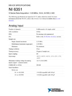
NI 6351 Device Specifications - National Instruments
www.ni.comSlew rate 20 V/μs Glitch energy at midscale transition, ±10 V range 10 nV · s External Reference APFI 0 characteristics Input impedance 10 kΩ Coupling DC Protection, device on ±30 V Protection, device off ±15 V Range ±11 V Slew rate 20 V/μs 1 Typical behavior. Time period may be longer due to host system USB performance. Time period