
BSS138 - N-Channel Logic Level Enhancement Mode Field ...
Enhancement Mode Field Effect Transistor BSS138 General Description These N−Channel enhancement mode field effect transistors are produced using onsemi’s proprietary, high cell density, DMOS ... R JA is the sum of the junction−to−case and case−to−ambient thermal resistance where the case thermal reference is defined as the solder
Download BSS138 - N-Channel Logic Level Enhancement Mode Field ...
Information
Domain:
Source:
Link to this page:
Documents from same domain

BCP56T1 - NPN Silicon Epitaxial Transistor
www.onsemi.com© Semiconductor Components Industries, LLC, 2016 March, 2018 − Rev. 14 1 Publication Order Number: BCP56T1/D BCP56 Series NPN Silicon Epitaxial Transistor These NPN Silicon Epitaxial transistors are designed for use in

AN1040/D Mounting Considerations For Power …
www.onsemi.comSemiconductor Components Industries, LLC, 2001 May, 2001 – Rev. 3 1 Publication Order Number: AN1040/D AN1040/D Mounting Considerations For Power Semiconductors

Corporate Fact Sheet - ON Semiconductor
www.onsemi.comCompany Profile ON Semiconductor (Nasdaq: ON) is driving energy efficient innovations, empowering customers to reduce global energy use. The company is a leading supplier of semiconductor-based

AND8231 - Circuit Configuration Options for TVS …
www.onsemi.comAND8231/D www.onsemi.com 2 Avalanche TVS Diodes Avalanche diodes are a good TVS device for applications that require power line surge immunity and ESD protection.

BCP53 Series PNP Silicon Epitaxial Transistors
www.onsemi.comBCP53 Series www.onsemi.com 3 TYPICAL CHARACTERISTICS Figure 1. Collector Emitter Saturation Voltage vs. Collector Current Figure 2. DC Current Gain vs. Collector

AND8299 - EMC Tests and PCB Guidelines for …
www.onsemi.comAND8299 - EMC Tests and PCB Guidelines for Automotive Linear Regulators

BSS138 N-Channel Logic Level Enhancement Mode …
www.onsemi.com2005 Semiconductor Components Industries, LLC. September-2017, Rev. 3 Publication Order Number: BSS138/D BSS138 N-Channel Logic Level Enhancement Mode Field Effect Transistor

TND310 ON Semiconductor Device Nomenclature
www.onsemi.comThis document contains the device nomenclature breakdown (also referred to as the part number decoder, product naming convention, or part naming convention) for …

LP2950 - 100 mA, Low Power Low Dropout Voltage …
www.onsemi.comLP2950, LP2951, NCV2951 www.onsemi.com Dropout Voltage V 0 in LP2950/LP2951 BIAS CURRENT (mA) I = 25°C V

2018 PHILIPPINES BENEFITS SUMMARY - ON …
www.onsemi.com2018 PHILIPPINES BENEFITS SUMMARY Employees are eligible for most benefits program on the first day of employment. Holidays: Ten (10) paid national regular holidays and Eight (8) national special holidays per year as provided
Related documents

FQP30N06L 60V LOGIC N-Channel MOSFET - SparkFun …
cdn.sparkfun.comThese N-Channel enhancement mode power field effect transistors are produced using Fairchild’s proprietary, planar stripe, DMOS technology. This advanced technology has been especially tailored to minimize on-state resistance, provide superior switching performance, and withstand high energy pulse in the avalanche and commutation mode.
Chapter 29 – Electromagnetic Induction
physics.ucf.edu1) The magnetic field created by the induced current in a metallic sample due to time-fluctuation of the external magnetic field of the coil wants to avoid its cause (i.e., the coil's fluctuating magnetic field). 2) Thus, the induced magnetic field in the sample and the external fluctuating magnetic field of the coil repel each other.
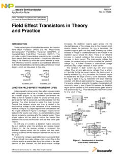
Field Effect Transistors in Theory and Practice ...
www.nxp.comJUNCTION FIELD-EFFECT TRANSISTOR (JFET) Inits simplest formthejunctionfield-effect transistorstarts with nothing more than a bar of doped silicon that behaves as a resistor (Figure 1a). By convention, the terminal into which current is injected is called the source terminal, since, as far as the FET is concerned, current originates from this ...

Field Effect Transistors - Learn About Electronics
learnabout-electronics.orgField Effect Transistors Module 4.1 Junction Field Effect Transistors Field Effect Transistors Although there are lots of confusing names for field effect transistors (FETs) there are basically two main types: 1. The reverse biased PN junction types, the JFET or Junction FET, (also called the JUGFET or Junction Unipolar Gate FET). 2.
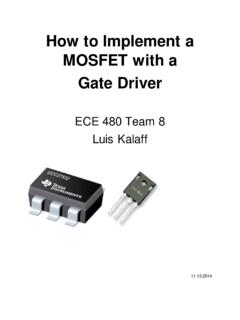
How to Implement a MOSFET with a Gate Driver
www.egr.msu.eduNov 13, 2014 · Frequency, Junction. Introduction A MOSFET is an acronym for metal-oxide semiconductor field-effect transistor. It is a special type of field-effect transistor (FET) and is the key component in high frequency, high efficiency switching applications across the electronics industry. A MOSFET is a voltage controlled device.

Bipolar Junction Transistor (BJT) Basics- GATE Problems
www.gatestudy.com(a) Bipolar junction transistors (b) NMOS transistors (c) Unipolar junction transistors (d) Junction field – effect transistors [GATE 1995] Soln. Ebers Moll model is one of classical models of BJT for small signals. This model is based on interacting diode junctions and is applicable to any transistor operating modes Option (a)
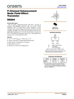
BSS84 - P-Channel Enhancement Mode Field-Effect Transistor
www.onsemi.comThis P−channel enhancement−mode field−effect transistor is produced using onsemi’s proprietary, high cell density, DMOS technology. This very high density process minimizes on−state ... R JA is the sum of the junction−to−case and case−to−ambient thermal resistance where the case thermal reference is defined as the solder

Chapter 2 Semiconductor Heterostructures - Cornell …
courses.cit.cornell.eduexactly zero in the depletion regions of thicknesses xp and xn on the p-side and n-side of the junction, respectively. It is a good approximation to calculate the junction electric field and potential. The net charge density in the depletion regions is then due to the ionized donors and acceptors and is as shown below.