
LM339 - Single Supply Quad Comparators
• Low Input Bias Current: 25 nA (Typ) • Low Input Offset Current: ±5.0 nA (Typ) • Low Input Offset Voltage • Input Common Mode Voltage Range to GND • Low Output Saturation Voltage: 130 mV (Typ) @ 4.0 mA • TTL and CMOS Compatible • ESD Clamps on the Inputs Increase Reliability without Affecting Device Operation
Download LM339 - Single Supply Quad Comparators

Information
Domain:
Source:
Link to this page:
Documents from same domain

BCP56T1 - NPN Silicon Epitaxial Transistor
www.onsemi.com© Semiconductor Components Industries, LLC, 2016 March, 2018 − Rev. 14 1 Publication Order Number: BCP56T1/D BCP56 Series NPN Silicon Epitaxial Transistor These NPN Silicon Epitaxial transistors are designed for use in

AN1040/D Mounting Considerations For Power …
www.onsemi.comSemiconductor Components Industries, LLC, 2001 May, 2001 – Rev. 3 1 Publication Order Number: AN1040/D AN1040/D Mounting Considerations For Power Semiconductors

Corporate Fact Sheet - ON Semiconductor
www.onsemi.comCompany Profile ON Semiconductor (Nasdaq: ON) is driving energy efficient innovations, empowering customers to reduce global energy use. The company is a leading supplier of semiconductor-based

AND8231 - Circuit Configuration Options for TVS …
www.onsemi.comAND8231/D www.onsemi.com 2 Avalanche TVS Diodes Avalanche diodes are a good TVS device for applications that require power line surge immunity and ESD protection.

BCP53 Series PNP Silicon Epitaxial Transistors
www.onsemi.comBCP53 Series www.onsemi.com 3 TYPICAL CHARACTERISTICS Figure 1. Collector Emitter Saturation Voltage vs. Collector Current Figure 2. DC Current Gain vs. Collector

AND8299 - EMC Tests and PCB Guidelines for …
www.onsemi.comAND8299 - EMC Tests and PCB Guidelines for Automotive Linear Regulators

BSS138 N-Channel Logic Level Enhancement Mode …
www.onsemi.com2005 Semiconductor Components Industries, LLC. September-2017, Rev. 3 Publication Order Number: BSS138/D BSS138 N-Channel Logic Level Enhancement Mode Field Effect Transistor

TND310 ON Semiconductor Device Nomenclature
www.onsemi.comThis document contains the device nomenclature breakdown (also referred to as the part number decoder, product naming convention, or part naming convention) for …

LP2950 - 100 mA, Low Power Low Dropout Voltage …
www.onsemi.comLP2950, LP2951, NCV2951 www.onsemi.com Dropout Voltage V 0 in LP2950/LP2951 BIAS CURRENT (mA) I = 25°C V

2018 PHILIPPINES BENEFITS SUMMARY - ON …
www.onsemi.com2018 PHILIPPINES BENEFITS SUMMARY Employees are eligible for most benefits program on the first day of employment. Holidays: Ten (10) paid national regular holidays and Eight (8) national special holidays per year as provided
Related documents
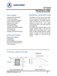
AEROSEMI - Olimex
www.olimex.comInput and Output capacitors should be placed close to the IC and connected to ground plane to reduce noise coupling. The GND should be connected to a strong ground plane for heat sinking and noise protection. Keep the main current traces as possible as short and wide. SW node of DC-DC converter is with high frequency voltage swing.

LF353-NWide Bandwidth Dual JFET Input Operational Amplifier
www.ti.com• Fast Settling Time to 0.01%: 2 μs input offset voltage, low input bias current, high input impedance, high slew rate and wide bandwidth. The devices also exhibit low noise and offset voltage drift. Typical Connection 1 Please be aware that an important notice concerning availability, standard warranty, and use in critical applications of

KAAP686 Mathematics and Signal Processing for …
www1.udel.eduApr 27, 2011 · The rectified signal is low pass filtered, with in the 5 – 100 Hz range, and the result looks like the “envelope” of the original signal. One way to low pass filter a signal is to simply take the mean value, in a window which “slides” along the signal. Some authors advocate this “rectify and mean” approach. Such a moving–average
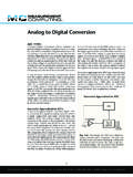
Analog to Digital Conversion - mccdaq.com
www.mccdaq.cominput of 10 VDC can resolve the measurement into 10 VDC/4096 = 0.00244 VDC = 2.44 mV. Similarly, for the same 0 to 10 VDC range, a 16-bit ADC resolution is 10/216 = 10/65,536 = 0.153 mV. The resolution is usually specified with respect to the full-range reading of the ADC, not with respect to the measured value at any particular instant.
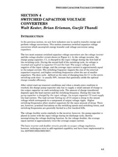
SECTION 4 SWITCHED CAPACITOR VOLTAGE CONVERTERS …
www.analog.comSwitched capacitor voltage converters do not maintain high efficiency for a wide range of ratios of input to output voltages, unlike their switching regulator counterparts. Because the input to output current ratio is scaled according to the basic voltage conversion (i.e., doubled for a doubler, inverted for an inverter)
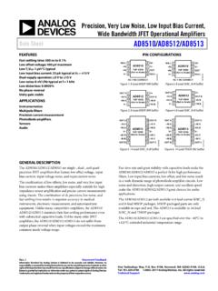
Precision, Very Low Noise, Low Input Bias Current, Wide ...
www.analog.comoutput phase reversal when input voltages exceed the maximum common-mode voltage range. Fast slew rate and great stability with capacitive loads make the AD8510/AD8512/AD8513 a perfect fit for high performance filters. Low input bias currents, low offset, and low noise result in a wide dynamic range of photodiode amplifier circuits. Low
ICM7555 General purpose CMOS timer
www.nxp.comn Wide operating supply voltage range guaranteed 3 V to 16 V over full automotive temperatures n Normal reset function; no crowbarring of supply during output transition ... VI input voltage TRIGGER: VDD = 5 V 0.29VDD 0.31VDD 0.34VDD V CONTROL_VOLTAGE: VDD = 5 V 0.62VDD 0.65VDD 0.67VDD V THRESHOLD: ...

LM2576 - 3.0 A, 15 V, Step-Down Switching Regulator
www.onsemi.com• Adjustable Version Output Voltage Range, 1.23 to 37 V ±4% Maximum Over Line and Load Conditions • Guaranteed 3.0 A Output Current • Wide Input Voltage Range • Requires Only 4 External Components • 52 kHz Fixed Frequency Internal Oscillator • TTL Shutdown Capability, Low Power Standby Mode • High Efficiency