Transcription of ADuCM360/ADuCM361 Hardware User Guide UG …
1 ADuCM360/ADuCM361 Hardware user Guide UG-367. One Technology Way Box 9106 Norwood, MA 02062-9106, Tel: Fax: Using the ADuCM360/ADuCM361 Low Power, Precision Analog Microcontroller with Dual Sigma-Delta ADCs, ARM Cortex-M3. SCOPE. This user Guide provides a detailed description of the ADuCM360/ADuCM361 functionality and features. DISCLAIMER. Information furnished by Analog Devices, Inc., is believed to be accurate and reliable. However, no responsibility is assumed by Analog Devices for its use, nor any infringements of patents or other rights of third parties that may result from its use.
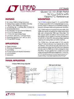
2 Specifications subject to change without notice. No license is granted by implication or otherwise under any patent or patent rights of Analog Devices. Trademarks and registered trademarks are the property of their respective owners. 12-BIT ON-CHIP ON-CHIP. DAC BUFFER ANALOG DIGITAL POWER-ON RESET. DAC RESET. AVDD LDO LDO. VBIAS. AGND. GENERATOR. ON-CHIP XTALO. OSCILLATOR. (1% TYPICAL). 16 MHz XTALI. VREF 24-BIT ARM. AIN0 - ADC CORTEX-M3. AIN1 PROCESSOR. AIN2 - GPIO PORTS. AMP BUF MOD2 SINC3/4 16 MHz UART PORTS. AIN3 GAIN MODULATOR FILTER 2 SPI PORTS.
3 AIN4/IEXC I2C PORTS. AIN5/IEXC. TIMER0 19 GENERAL- AIN6/IEXC SINC2 MEMORY TIMER1 PURPOSE. AIN7/VBIAS0/IEXC/ MUX FILTER 128kB FLASH WATCHDOG I/O PORTS. EXTREF2IN+ 8kB SRAM WAKE-UP TIMER. PWM. AIN8/EXTREF2IN VREF 24-BIT. AIN9/DACBUFF+ - ADC SERIAL WIRE. DMA AND DEBUG, AIN10 INTERRUPT PROGRAMMING. AIN11/VBIAS1 MOD2 - SINC3/4 CONTROLLER AND DEBUG. AMP BUF. GAIN MODULATOR FILTER. SELECTABLE. DAC, TEMP, VREF SWDIO. IOVDD/4, SOURCES. AVDD/4 SWCLK. PRECISION. REFERENCE. aducm360 . DVDD_REG. IREF CURRENT BUFFER. SOURCES AVDD_REG. BUFFER.
4 10464-001. GND_SW VREF VREF+ INT_REF IOVDD IOVDD. Figure 1. aducm360 Block Diagram PLEASE SEE THE LAST PAGE FOR AN IMPORTANT. WARNING AND LEGAL TERMS AND CONDITIONS. Rev. D | Page 1 of 176. ADuCM360/ADuCM361 Hardware user Guide UG-367. TABLE OF CONTENTS. Scope .. 1 System Exceptions and Peripheral 56. Disclaimer .. 1 Cortex-M3 and Fault Management .. 56. Revision History .. 4 External Interrupt Configuration .. 59. Using the ADuCM360/ADuCM361 Hardware user Guide .. 5 Interrupt Memory Mapped Registers .. 59. Number Notations.
5 5 DMA Controller .. 64. Register Access Conventions .. 5 DMA Features .. 64. Acronyms and Abbreviations .. 5 DMA Overview .. 64. Introduction to the ADuCM360/ADuCM361 .. 6 DMA Operation .. 64. Main Features of ADuCM360/ADuCM361 .. 7 Error Management .. 64. Memory Organization .. 9 Interrupts .. 64. Clocking Architecture .. 10 DMA Priority .. 65. Clocking Architecture Features .. 10 Channel Control Data Structure .. 65. Clocking Architecture Block Diagram .. 10 Control Data Configuration .. 66. Clocking Architecture 11 DMA Transfer Types (CHNL_CFG[2:0]).
6 67. Clocking Architecture 11 Address Calculation .. 69. Clocking Architecture Memory Mapped Registers .. 11 DMA Memory Mapped Registers .. 72. Power Management Unit .. 15 Flash Controller .. 86. Power Management Unit Features .. 15 Flash Controller Features .. 86. Power Management Unit 15 Flash Controller Overview .. 86. Power Management Unit Operation .. 15 Flash Memory Organization .. 86. Power Management Unit Memory Mapped Registers .. 16 Writing to Flash/EE Memory .. 87. Cortex-M3 Processor .. 18 Erasing Flash/EE Memory.
7 87. Cortex-M3 Processor Features .. 18 Flash Controller Performance and Command Duration .. 88. Cortex-M3 Processor Overview .. 18 Flash Protection .. 88. Cortex-M3 Processor Operation .. 18 Flash Controller Failure Analysis Key .. 89. Related Documents .. 19 Flash Integrity Signature Feature .. 89. ADC Circuit .. 20 Integrity of the 89. ADC Circuit Features .. 20 Abort Using Interrupts .. 89. ADC Circuit Block 20 Flash Controller Memory Mapped Registers .. 90. ADC Circuit Overview .. 20 Reset .. 99. ADC Circuit Operation.
8 21 Reset Features .. 99. Other ADC Support Circuits .. 25 Reset Operation .. 99. Other ADC 28 Reset Memory Mapped Registers .. 100. ADC Circuit Memory Mapped Registers .. 35 Digital I/Os .. 101. DAC .. 51 Digital I/Os Features .. 101. DAC Features .. 51 Digital I/Os Block Diagram .. 101. DAC 51 Digital I/Os 101. DAC Operation .. 51 Digital I/Os 101. DAC DMA 53 Digital Port Multiplex .. 103. DAC Memory Mapped Registers .. 54 GPIO Memory Mapped 104. Rev. D | Page 2 of 176. UG-367 ADuCM360/ADuCM361 Hardware user Guide I2C Serial Interface.
9 107 General-Purpose Timers Overview ..147. I2C Features .. 107 General-Purpose Timers Operation ..147. I2C 107 General-Purpose Timers Memory Mapped Registers ..149. I C 107. 2. Wake-Up Timer ..153. I C Operating Modes .. 109. 2. Wake-Up Timer Features ..153. I C Memory Mapped Registers .. 116. 2. Wake-Up Timer Block Diagram ..153. Serial Peripheral Interfaces .. 125 Wake-Up Timer Overview ..153. SPI Features .. 125 Wake-Up Timer Operation ..153. SPI Overview .. 125 Wake-Up Timer Memory Mapped Registers ..155. SPI Operation.
10 125 Watchdog SPI Transfer Initiation .. 126 Watchdog Timer Features ..160. SPI Interrupts .. 128 Watchdog Timer Block Diagram ..160. Wire-OR'ed Mode (WOM) .. 128 Watchdog Timer Overview ..160. CSERR Condition .. 129 Watchdog Timer Operation ..160. SPI1 DMA .. 129 Watchdog Timer Memory Mapped Registers ..161. SPI and Power-Down Modes .. 133 PWM ..163. SPI Memory Mapped Registers .. 133 PWM Features ..163. UART Serial Interface .. 138 PWM Overview ..163. UART Features .. 138 PWM Operation ..163. UART Overview .. 138 PWM Interrupt Generation.