Transcription of BAT54HT1 - Schottky Barrier Diodes - ON …
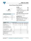
1 Semiconductor Components Industries, LLC, 2014 December, 2014 Rev. 71 Publication Order Number: BAT54HT1 /DBAT54 HSchottky Barrier DiodesThese Schottky Barrier Diodes are designed for high speed switchingapplications, circuit protection, and voltage clamping. Extremely lowforward voltage reduces conduction loss. Miniature surface mountpackage is excellent for hand held and portable applications wherespace is Extremely Fast Switching Speed Low Forward Voltage V (Typ) @ IF = 10 mAdc Device Marking: JV NSV Prefix for Automotive and Other Applications RequiringUnique Site and Control Change Requirements; AEC Q101 Qualified and PPAP Capable These Devices are Pb Free, Halogen Free/BFR Free and are RoHSCompliant*MAXIMUM RATINGS (TJ = 125 C unless otherwise noted)RatingSymbolValueUnitReverse VoltageVR30 VStresses exceeding those listed in the Maximum Ratings table may damage thedevice.
2 If any of these limits are exceeded, device functionality should not beassumed, damage may occur and reliability may be CHARACTERISTICSC haracteristicSymbolMaxUnitTotal Device Dissipation FR 5 Board,(Note 1)TA = 25 CDerate above 25 CForward Current (DC)IF200 MaxmANon Repetitive Peak Forward Current, tp < 10 msecIFSM600mARepetitive Peak Forward CurrentPulse Wave = 1 sec, Duty Cycle = 66%IFRM300mAThermal Resistance Junction to AmbientRqJA635 C/WJunction and Storage Temperature RangeTJ, Tstg 55to150 C1. FR 4 Minimum Pad*For additional information on our Pb Free strategy and soldering details, pleasedownload the ON Semiconductor Soldering and Mounting TechniquesReference Manual, VOLT SILICONHOT CARRIER DETECTORAND SWITCHING DIODESD evicePackageShipping ORDERING INFORMATIONSOD 323 CASE 477 STYLE 11 CATHODE2 ANODEMARKING 323(Pb Free)3,000 / Tape & Reel For information on tape and reel specifications,including part orientation and tape sizes, pleaserefer to our Tape and Reel Packaging SpecificationsBrochure, BRD8011 Device CodeM= Date CodeG= Pb Free Package(Note.)
3 Microdot may be in either location)NSVBAT54HT1 GSOD 323(Pb Free)3,000 / Tape & CHARACTERISTICS (TA = 25 C unless otherwise noted)CharacteristicSymbolMinTypMaxUnitR everse Breakdown Voltage(IR = 10 A)V(BR)R30 VTotal Capacitance(VR = V, f = MHz)CT Leakage(VR = 25 V)IR AdcForward Voltage(IF = mA)(IF = mA)(IF = 10 mA)(IF = 30 mA)(IF = 100 mA)VF Recovery Time(IF = IR = 10 mAdc, IR(REC) = mAdc) Figure 1trr : 1. A k variable resistor adjusted for a Forward Current (IF) of 10 : 2. Input pulse is adjusted so IR(peak) is equal to 10 : 3. tp trr+10 V2 k820 FDUTVR100 F50 OutputPulseGenerator50 InputSamplingOscilloscopetrtpt10%90%IFIR trrtiR(REC) = 1 mAOUTPUT PULSE(IF = IR = 10 mA; measuredat iR(REC) = 1 mA)IFINPUT SIGNALF igure 1. Recovery Time Equivalent Test , FORWARD VOLTAGE (VOLTS) C100VR, REVERSE VOLTAGE (VOLTS) , REVERSE VOLTAGE (VOLTS)124205101530 Figure 2.
4 Forward VoltageFigure 3. Leakage CurrentFigure 4. Total Capacitance 40 C25 CTA = 150 CTA = 125 CTA = 85 CTA = 25 55 C150 C125 C10010003025206810IR, REVERSE CURRENT ( A)IF, FORWARD CURRENT (mA)CT, TOATAL CAPACITANCE (pF) DIMENSIONSHESOD 323 CASE 477 02 ISSUE HNOTES:1. DIMENSIONING AND TOLERANCING PER , CONTROLLING DIMENSION: LEAD THICKNESS SPECIFIED PER L/F DRAWINGWITH SOLDER DIMENSIONS A AND B DO NOT INCLUDE MOLDFLASH, PROTRUSIONS OR GATE DIMENSION L IS MEASURED FROM END OF 3D12bEA3A1 ACNOTE *For additional information on our Pb Free strategy and solderingdetails, please download the ON Semiconductor Soldering andMounting Techniques Reference Manual, FOOTPRINT*STYLE 1:PIN 1. CATHODE (POLARITY BAND)2.
5 ANODEON Semiconductor and are registered trademarks of Semiconductor Components Industries, LLC (SCILLC). SCILLC reserves the right to make changes without further noticeto any products herein. SCILLC makes no warranty, representation or guarantee regarding the suitability of its products for any particular purpose, nor does SCILLC assume any liabilityarising out of the application or use of any product or circuit, and specifically disclaims any and all liability, including without limitation special, consequential or incidental damages. Typical parameters which may be provided in SCILLC data sheets and/or specifications can and do vary in different applications and actual performance may vary over time. Alloperating parameters, including Typicals must be validated for each customer application by customer s technical experts.
6 SCILLC does not convey any license under its patent rightsnor the rights of others. SCILLC products are not designed, intended, or authorized for use as components in systems intended for surgical implant into the body, or other applicationsintended to support or sustain life, or for any other application in which the failure of the SCILLC product could create a situation where personal injury or death may occur. ShouldBuyer purchase or use SCILLC products for any such unintended or unauthorized application, Buyer shall indemnify and hold SCILLC and its officers, employees, subsidiaries, affiliates,and distributors harmless against all claims, costs, damages, and expenses, and reasonable attorney fees arising out of, directly or indirectly, any claim of personal injury or deathassociated with such unintended or unauthorized use, even if such claim alleges that SCILLC was negligent regarding the design or manufacture of the part.
7 SCILLC is an EqualOpportunity/Affirmative Action Employer. This literature is subject to all applicable copyright laws and is not for resale in any ORDERING INFORMATIONN. American Technical Support: 800 282 9855 Toll FreeUSA/CanadaEurope, Middle East and Africa Technical Support:Phone: 421 33 790 2910 Japan Customer Focus CenterPhone: 81 3 5817 1050 BAT54HT1 /DLITERATURE FULFILLMENT:Literature Distribution Center for ON Box 5163, Denver, Colorado 80217 USAP hone: 303 675 2175 or 800 344 3860 Toll Free USA/CanadaFax: 303 675 2176 or 800 344 3867 Toll Free USA/CanadaEmail: Semiconductor Website: Literature: additional information, please contact your localSales Representativ