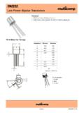
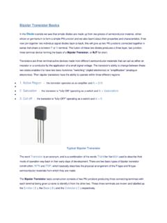
Transcription of BD135 - Plastic Medium-Power Silicon NPN Transistors
1 Semiconductor Components Industries, LLC, 2013 December, 2013 Rev. 171 Publication Order Number: BD135 /DBD135G, BD137G, BD139 GPlastic medium -PowerSilicon NPN TransistorsThis series of Plastic , medium power Silicon NPN Transistors aredesigned for use as audio amplifiers and drivers utilizingcomplementary or quasi complementary High DC Current Gain BD 135, 137, 139 are complementary with BD 136, 138, 140 These Devices are Pb Free, Halogen Free/BFR Free and are RoHSCompliant*MAXIMUM RATINGSR atingSymbolValueUnitCollector Emitter VoltageBD135 GBD137 GBD139 GVCEO456080 VdcCollector Base VoltageBD135 GBD137 GBD139 GVCBO4560100 VdcEmitter Base Device Dissipation@ TA = 25 CDerate above 25 CTotal Device Dissipation@ TC = 25 CDerate above 25 COperating and Storage JunctionTemperature RangeTJ, Tstg 55 to + 150 CStresses exceeding those listed in the Maximum Ratings table may damage thedevice. If any of these limits are exceeded, device functionality should not beassumed, damage may occur and reliability may be CHARACTERISTICSC haracteristicSymbolMaxUnitThermal Resistance, Junction to CaseRqJC10 C/WThermal Resistance, Junction to AmbientRqJA100 C/W*For additional information on our Pb Free strategy and soldering details, pleasedownload the ON Semiconductor Soldering and Mounting TechniquesReference Manual, A power TRANSISTORSNPN SILICON45, 60, 80 V, WY= YearWW= Work WeekBD1xx = Device Codexx = 35, 37, 39G= Pb Free PackageBD139 GTO 225(Pb Free)500 Units / BoxMARKING DIAGRAMBD135 TGTO 225(Pb Free)50 Units / RailBD135 GTO 225(Pb Free)500 Units / BoxBD137 GTO 225(Pb Free)500 Units / BoxORDERING INFORMATION3 BASE1 EMITTERCOLLECTOR2, 4TO 225 CASE 77 09 STYLE 1123 YWWBD1xxGBD135G, BD137G, BD139 CHARACTERISTICS (TC = 25_C unless otherwise noted)
2 CharacteristicSymbolMinMaxUnItCollector Emitter Sustaining Voltage*(IC = Adc, IB = 0) BD135 GBD137 GBD139 GBVCEO*456080 VdcCollector Cutoff Current(VCB = 30 Vdc, IE = 0)(VCB = 30 Vdc, IE = 0, TC = 125_C)ICBO Cutoff Current(VBE = Vdc, IC = 0)IEBO 10mAdcDC Current Gain(IC = A, VCE = 2 V)(IC = A, VCE = 2 V)(IC = A VCE = 2 V)hFE*254025 250 Collector Emitter Saturation Voltage*(IC = Adc, IB = Adc)VCE(sat)* Emitter On Voltage*(IC = Adc, VCE = Vdc)VBE(on)* 1 VdcProduct parametric performance is indicated in the Electrical Characteristics for the listed test conditions, unless otherwise noted. Productperformance may not be indicated by the Electrical Characteristics if operated under different conditions.*Pulse Test: Pulse Width 300 ms, Duty Cycle CHARACTERISTICSF igure 1. DC Current GainFigure 2. Collector Emitter Saturation VoltageIC, COLLECTOR CURRENT (A)IC, COLLECTOR CURRENT (A) , DC CURRENT GAINVCE(sat), COLLECTOR EMITTERSATURATION VOLTAGE (V)VCE = 2 V150 C 55 C25 CIC/IB = 10150 C 55 C25 CBD135G, BD137G, BD139 CHARACTERISTICSF igure 3.
3 Base Emitter Saturation VoltageFigure 4. Base Emitter On VoltageIC, COLLECTOR CURRENT (A)IC, COLLECTOR CURRENT (A) 5. CapacitanceFigure 6. Active Region Safe Operating AreaVR, REVERSE VOLTAGE (V)VCE, COLLECTOR EMITTER VOLTAGE (V) (sat), BASE EMITTERSATURATION VOLTAGE (V)VBE(on), BASE EMITTER ON VOLTAGE (V)C, CAPACITANCE (pF)IC, COLLECTOR CURRENT (A)IC/IB = 10150 C 55 C25 CVCE = 2 V150 C 55 C25 Cf = 1 MHzCibCobBD135BD137BD139TJ = 125 Cdc5 msFigure 7. power DeratingTA, AMBIENT TEMPERATURE ( C) , power DISSIPATION (W) , BD137G, BD139 DIMENSIONSTO 225 CASE 77 09 ISSUE :1. DIMENSIONING AND TOLERANCING PERASME , CONTROLLING DIMENSION: NUMBER AND SHAPE OF LUGS VIEWBACK VIEWFRONT VIEWSIDE VIEW1233214 PIN 4 BACKSIDE TABSTYLE 1:PIN , Semiconductor and are registered trademarks of Semiconductor Components Industries, LLC (SCILLC). SCILLC owns the rights to a number of patents, trademarks,copyrights, trade secrets, and other intellectual property.
4 A listing of SCILLC s product/patent coverage may be accessed at SCILLC reserves the right to make changes without further notice to any products herein. SCILLC makes no warranty, representation or guarantee regarding the suitability of its products for anyparticular purpose, nor does SCILLC assume any liability arising out of the application or use of any product or circuit, and specifically disclaims any and all liability, including withoutlimitation special, consequential or incidental damages. Typical parameters which may be provided in SCILLC data sheets and/or specifications can and do vary in different applicationsand actual performance may vary over time. All operating parameters, including Typicals must be validated for each customer application by customer s technical experts. SCILLC does not convey any license under its patent rights nor the rights of others. SCILLC products are not designed, intended, or authorized for use as components in systems intended forsurgical implant into the body, or other applications intended to support or sustain life, or for any other application in which the failure of the SCILLC product could create a situation wherepersonal injury or death may occur.
5 Should Buyer purchase or use SCILLC products for any such unintended or unauthorized application, Buyer shall indemnify and hold SCILLC andits officers, employees, subsidiaries, affiliates, and distributors harmless against all claims, costs, damages, and expenses, and reasonable attorney fees arising out of, directly or indirectly,any claim of personal injury or death associated with such unintended or unauthorized use, even if such claim alleges that SCILLC was negligent regarding the design or manufactureof the part. SCILLC is an Equal Opportunity/Affirmative Action Employer. This literature is subject to all applicable copyright laws and is not for resale in any ORDERING INFORMATIONN. American Technical Support: 800 282 9855 Toll FreeUSA/CanadaEurope, Middle East and Africa Technical Support:Phone: 421 33 790 2910 Japan Customer Focus CenterPhone: 81 3 5817 1050BD135/DLITERATURE FULFILLMENT:Literature Distribution Center for ON Box 5163, Denver, Colorado 80217 USAP hone: 303 675 2175 or 800 344 3860 Toll Free USA/CanadaFax: 303 675 2176 or 800 344 3867 Toll Free USA/CanadaEmail: Semiconductor Website: Literature: additional information, please contact your localSales Representativ