Transcription of MBRS130LT3G, SBRS8130LT3G Schottky Power …
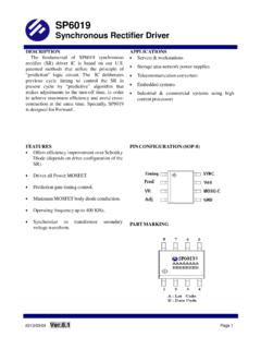
1 Semiconductor Components Industries, LLC, 2012 May, 2017 Rev. 101 Publication Order Number:MBRS130LT3/DMBRS130LT3G,SBRS8130L T3 GSchottky Power RectifierSurface Mount Power PackageThis device employs the Schottky Barrier principle in a large areametal to silicon Power diode. State of the art geometry featuresepitaxial construction with oxide passivation and metal overlaycontact. Ideally suited for low voltage, high frequency rectification,or as free wheeling and polarity protection diodes, in surface mountapplications where compact size and weight are critical to Very Low Forward Voltage Drop ( Volts Max @ A, TJ = 25 C) Small Compact Surface Mountable Package with J Bend Leads Highly Stable Oxide Passivated Junction Guard Ring for Stress Protection ESD Ratings: Human Body Model = 3B (> 16000 V) Machine Model = C (> 400 V) SBRS8 Prefix for Automotive and Other Applications RequiringUnique Site and Control Change Requirements.
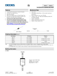
2 AEC Q101 Qualified and PPAP Capable* These are Pb Free DevicesMechanical Characteristics Case: Epoxy, Molded Weight: 100 mg (approximately) Finish: All External Surfaces Corrosion Resistant and TerminalLeads are Readily Solderable Lead and Mounting Surface Temperature for Soldering Purposes:260 C Max. for 10 Seconds Cathode Polarity 403 ASCHOTTKY AMPERE30 VOLTSD evicePackageShipping ORDERING INFORMATIONMBRS130LT3 GSMB(Pb Free)2,500 / Tape & Reel For information on tape and reel specifications,including part orientation and tape sizes, pleaserefer to our Tape and Reel Packaging SpecificationsBrochure, BRD8011 DIAGRAM1BL3= Specific Device CodeA= Assembly Location**Y= YearWW= Work WeekG= Pb Free PackageAYWW1BL3 GGSBRS8130LT3G*SMB(Pb Free)2,500 / Tape & ReelSBRS8130LT3G VF01* SMB(Pb Free)2,500 / Tape & Reel**The Assembly Location code (A) is front sideoptional.
3 In cases where the Assembly Location isstamped in the package bottom (molding ejecter pin),the front side assembly code may be blank.(Note: Microdot may be in either location) mbrs130lt3g , RATINGSR atingSymbolValueUnitPeak Repetitive Reverse VoltageWorking Peak Reverse VoltageDC Blocking VoltageVRRMVRWMVR30 VAverage Rectified Forward CurrentTL = 120 CTL = 110 CIF(AV) Repetitive Peak Surge Current(Surge Applied at Rated Load Conditions Halfwave, Single Phase, 60 Hz)IFSM40 AOperating Junction TemperatureTJ 65 to +125 CStresses exceeding those listed in the Maximum Ratings table may damage the device. If any of these limits are exceeded, device functionalityshould not be assumed, damage may occur and reliability may be CHARACTERISTICSC haracteristicSymbolValueUnitThermal Resistance,Junction to LeadYJL12 C/WThermal Resistance,Junction to Ambient (TA = 25 C, Min Pad, 1 oz copper)Junction to Ambient (TA = 25 C, 1 Pad, 1 oz copper) C/WELECTRICAL CHARACTERISTICSC haracteristicSymbolValueUnitMaximum Instantaneous Forward Voltage (Note 1)(iF = A, TJ = 25 C)(iF = A, TJ = 25 C) Instantaneous Reverse Current (Note 1)(Rated dc Voltage, TJ = 25 C)(Rated dc Voltage, TJ = 100 C) parametric performance is indicated in the Electrical Characteristics for the listed test conditions, unless otherwise noted.
4 Productperformance may not be indicated by the Electrical Characteristics if operated under different Pulse Test: Pulse Width = 300 ms, Duty Cycle 2%.VF, INSTANTANEOUS VOLTAGE (V)Figure 1. Typical Forward VoltageFigure 2. Maximum Forward , INSTANTANEOUS FORWARD CURRENT(A)TJ = 100 C25 , MAXIMUM INSTANTANEOUS FORWARDCURRENT (A)TJ = 100 C25 CVF, MAXIMUM INSTANTANEOUS VOLTAGE (V) mbrs130lt3g , , REVERSE VOLTAGE (V)IR, IREVERSE CURRENT (mA)TJ = 100 C25 C036912151821242730VR, REVERSE VOLTAGE (V)IR, IREVERSE CURRENT (mA)TJ = 100 C25 CFigure 3. Typical Reverse Leakage CurrentFigure 4. Typical Maximum Reverse , CASE TEMPERATURE ( C)Figure 5. Current Derating (Case)IF(AV), AVERAGE FORWARD CURRENT (A)SQUARE (AV), AVERAGE FORWARD CURRENT (A)Figure 6. Typical Power DissipationPF(AV), AVERAGE Power DISSIPATION (W)SQUAREDCC, CAPACITANCE (pF)4003503002502001501005000 4 8 12162024 2832VR, REVERSE VOLTAGE (VOLTS)Figure 7.
5 Typical CapacitanceNOTE: TYPICAL CAPACITANCEAT 0 V = 290 pFMBRS130LT3G, 8. Thermal Response, Min Padt, TIME (s) = TRANSIENT THERMAL RESISTANCEF igure 9. Thermal Response, 1 Inch Padt, TIME (s) = TRANSIENT THERMAL RESISTANCEF igure 10. Thermal Resistance vs. Copper AreaFigure 11. Power Dissipation vs. Copper Area025507510012515017520022501002003004 00500600700 COPPER AREA (mm2)qJA ( C/W) AREA (mm2) Power DISSIPATION (W) based on TA = 25 CMBRS130LT3G, DIMENSIONSSMBCASE 403A 03 ISSUE JEbDcL1 LAA1 NOTES:1. DIMENSIONING AND TOLERANCING PER ANSI , CONTROLLING DIMENSION: DIMENSION b SHALL BE MEASURED WITHIN DIMENSION mminches SCALE 8:1*For additional information on our Pb Free strategy and solderingdetails, please download the ON Semiconductor Soldering andMounting Techniques Reference Manual, FOOTPRINT* REFDL1 HEPOLARITY INDICATOROPTIONAL AS NEEDEDON Semiconductor and are trademarks of Semiconductor Components Industries, LLC dba ON Semiconductor or its subsidiaries in the United States and/or other Semiconductor owns the rights to a number of patents, trademarks, copyrights, trade secrets, and other intellectual property.
6 A listing of ON Semiconductor s product/patent coveragemay be accessed at ON Semiconductor reserves the right to make changes without further notice to any products Semiconductor makes no warranty, representation or guarantee regarding the suitability of its products for any particular purpose, nor does ON Semiconductor assume any liabilityarising out of the application or use of any product or circuit, and specifically disclaims any and all liability, including without limitation special, consequential or incidental damages. Buyeris responsible for its products and applications using ON Semiconductor products, including compliance with all laws, regulations and safety requirements or standards, regardless ofany support or applications information provided by ON Semiconductor. Typical parameters which may be provided in ON Semiconductor data sheets and/or specifications can anddo vary in different applications and actual performance may vary over time.
7 All operating parameters, including Typicals must be validated for each customer application by customer stechnical experts. ON Semiconductor does not convey any license under its patent rights nor the rights of others. ON Semiconductor products are not designed, intended, or authorizedfor use as a critical component in life support systems or any FDA Class 3 medical devices or medical devices with a same or similar classification in a foreign jurisdiction or any devicesintended for implantation in the human body. Should Buyer purchase or use ON Semiconductor products for any such unintended or unauthorized application, Buyer shall indemnify andhold ON Semiconductor and its officers, employees, subsidiaries, affiliates, and distributors harmless against all claims, costs, damages, and expenses, and reasonable attorney feesarising out of, directly or indirectly, any claim of personal injury or death associated with such unintended or unauthorized use, even if such claim alleges that ON Semiconductor wasnegligent regarding the design or manufacture of the part.
8 ON Semiconductor is an Equal Opportunity/Affirmative Action Employer. This literature is subject to all applicable copyrightlaws and is not for resale in any ORDERING INFORMATIONN. American Technical Support: 800 282 9855 Toll FreeUSA/CanadaEurope, Middle East and Africa Technical Support:Phone: 421 33 790 2910 Japan Customer Focus CenterPhone: 81 3 5817 1050 MBRS130LT3/DLITERATURE FULFILLMENT:Literature Distribution Center for ON Semiconductor19521 E. 32nd Pkwy, Aurora, Colorado 80011 USAP hone: 303 675 2175 or 800 344 3860 Toll Free USA/CanadaFax: 303 675 2176 or 800 344 3867 Toll Free USA/CanadaEmail: Semiconductor Website: Literature: additional information, please contact your localSales Representative