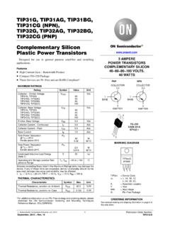
Transcription of MJE15032 - Complementary Silicon Plastic Power Transistors
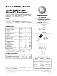
1 Semiconductor Components Industries, LLC, 2014 December, 2014 Rev. 61 Publication Order Number: MJE15032 /DMJE15032 (NPN),MJE15033 (PNP) Complementary SiliconPlastic Power TransistorsDesigned for use as high frequency drivers in audio High DC Current Gain High Current Gain Bandwidth Product TO 220 Compact Package Epoxy Meets UL 94 V 0 @ in These Devices are Pb Free and are RoHS Compliant*MAXIMUM RATINGSR atingSymbolValueUnitCollector Emitter VoltageVCEO250 VdcCollector Base VoltageVCB250 VdcEmitter Base Current Current PeakICM16 AdcBase Power Dissipation@ TC = 25_CDerate above Power Dissipation@ TA = 25_CDerate above and Storage JunctionTemperature RangeTJ, Tstg 65 to + 150_CESD Human Body ModelHBM3 BVESD Machine ModelMMCVS tresses exceeding those listed in the Maximum Ratings table may damage thedevice. If any of these limits are exceeded, device functionality should not beassumed, damage may occur and reliability may be CHARACTERISTICSC haracteristicSymbolMaxUnitThermal Resistance,Junction to Resistance,Junction to *For additional information on our Pb Free strategy and soldering details, pleasedownload the ON Semiconductor Soldering and Mounting TechniquesReference Manual, INFORMATIONTO 220 CASE 221 ASTYLE 1 MARKINGDIAGRAMMJE1503x = Specific Device Codex= 2 or 3A= Assembly LocationY= YearWW= Work WeekG= Pb Free AMPERESPOWER TRANSISTORSCOMPLEMENTARY SILICON250 VOLTS, 50 WATTS1234 MJE1503xGAYWWMJE15032 GTO 220(Pb Free)50 Units/RailMJE15033 GTO 220(Pb Free)50 Units/RailCOMPLEMENTARY1 BASE3 EMITTERCOLLECTOR2, 41 BASE3 EMITTERCOLLECTOR2, 4 MJE15032 (NPN), MJE15033 (PNP) CHARACTERISTICS (TC = 25_C unless otherwise noted)
2 CharacteristicSymbolMinMaxUnitOFF CHARACTERISTICSC ollector Emitter Sustaining Voltage (Note 1)(IC = 10 mAdc, IB = 0)VCEO(sus)250 VdcCollector Cutoff Current(VCB = 250 Vdc, IE = 0)ICBO 10mAdcEmitter Cutoff Current(VBE = Vdc, IC = 0)IEBO 10mAdcON CHARACTERISTICS (Note 1)DC Current Gain(IC = Adc, VCE = Vdc)(IC = Adc, VCE = Vdc)(IC = Adc, VCE = Vdc)hFE705010 Collector Emitter Saturation Voltage(IC = Adc, IB = Adc)VCE(sat) Emitter On Voltage(IC = Adc, VCE = Vdc)VBE(on) CHARACTERISTICSC urrent Gain Bandwidth Product (Note 2)(IC = 500 mAdc, VCE = 10 Vdc, ftest = MHz)fT30 MHzProduct parametric performance is indicated in the Electrical Characteristics for the listed test conditions, unless otherwise noted. Productperformance may not be indicated by the Electrical Characteristics if operated under different Pulse Test: Pulse Width 300 ms, Duty Cycle fT = hfe (NPN), MJE15033 (PNP) , TIME (ms) (t), TRANSIENT THERMALZqJC(t) = r(t) RqJCRqJC = C/W MAXD CURVES APPLY FOR POWERPULSE TRAIN SHOWNREAD TIME AT t1TJ(pk) - TC = P(pk) ZqJC(t)P(pk)t1t2 DUTY CYCLE, D = t1 PULSERESISTANCE (NORMALIZED)Figure 1.
3 Thermal = ms100 ms50 ms10 2. MJE15032 & MJE15033 Safe Operating AreaVCE, COLLECTOR-EMITTER VOLTAGE (VOLTS) , COLLECTOR CURRENT (AMPS) are two limitations on the Power handling ability ofa transistor: average junction temperature and secondbreakdown. Safe operating area curves indicate IC VCElimits of the transistor that must be observed for reliableoperation, , the transistor must not be subjected to greaterdissipation then the curves data of Figures 2 and 4 is based on TJ(pk) = 150_C;TC is variable depending on conditions. Second breakdownpulse limits are valid for duty cycles to 10% provided TJ(pk)< 150_C. TJ(pk) may be calculated from the data in Figure high case temperatures, thermal limitations will reducethe Power that can be handled to values less than thelimitations imposed by second 3. Power DeratingT, TEMPERATURE ( C)0406010012016040TC2060PD, Power DISSIPATION (WATTS) (NPN), MJE15033 (PNP) C150 C-55 4.
4 NPN MJE15032 VCE = 5 V DC Current GainIC, COLLECTOR CURRENT (AMPS) , DC CURRENT 5. PNP MJE15033 VCE = 5 V DC Current GainFigure 6. NPN MJE15032 VCE = 5 V VBE(on) CurveIC, COLLECTOR CURRENT (AMPS) , VOLTAGE (VOLTS) 7. PNP MJE15033 VCE = 5 V VBE(on) CurveIC, COLLECTOR CURRENT (AMPS)10V, VOLTAGE (VOLTS) MJE15032 PNP MJE1503325 C150 C-55 C25 C150 C-55 , COLLECTOR CURRENT (AMPS) , DC CURRENT C150 C-55 CIC, COLLECTOR CURRENT (AMPS)IC, COLLECTOR CURRENT (AMPS)V, VOLTAGE (VOLTS)Figure 8. NPN MJE15032 VCE(sat) IC/IB = 10 Figure 9. PNP MJE15033 VCE(sat) IC/IB = , VOLTAGE (VOLTS) C150 C-55 C25 C150 C-55 CMJE15032 (NPN), MJE15033 (PNP) , COLLECTOR CURRENT (AMPS) , VOLTAGE (VOLTS)NPN MJE15032 PNP MJE15033V, VOLTAGE (VOLTS)Figure 10. NPN MJE15032 VCE(sat) IC/IB = 20 Figure 11. PNP MJE15033 VCE(sat) IC/IB = , COLLECTOR CURRENT (AMPS) 12. NPN MJE15032 VBE(sat) IC/IB = 10 Figure 13.
5 PNP MJE15033 VBE(sat) IC/IB = C150 C-55 CIC, COLLECTOR CURRENT (AMPS) C150 C-55 C, BASE EMITTER VOLTAGE (VOLTS) , COLLECTOR CURRENT (AMPS) , BASE EMITTER VOLTAGE (VOLTS)BE25 C150 C-55 C25 C150 C-55 CTO 220 CASE 221 AISSUE AKDATE 13 JAN 2022 SCALE 1:1 STYLE 1:PIN 1. BASE2. COLLECTOR3. EMITTER4. COLLECTORSTYLE 2:PIN 1. BASE2. EMITTER3. COLLECTOR4. EMITTERSTYLE 3:PIN 1. CATHODE2. ANODE3. GATE4. ANODESTYLE 4:PIN 1. MAIN TERMINAL 12. MAIN TERMINAL 23. GATE4. MAIN TERMINAL 2 STYLE 7:PIN 1. CATHODE2. ANODE3. CATHODE4. ANODESTYLE 10:PIN 1. GATE2. SOURCE3. DRAIN4. SOURCESTYLE 5:PIN 1. GATE2. DRAIN3. SOURCE4. DRAINSTYLE 8:PIN 1. CATHODE2. ANODE3. EXTERNAL TRIP/DELAY4. ANODESTYLE 6:PIN 1. ANODE2. CATHODE3. ANODE4. CATHODESTYLE 9:PIN 1. GATE2. COLLECTOR3. EMITTER4. COLLECTORSTYLE 11:PIN 1.
6 DRAIN2. SOURCE3. GATE4. SOURCESTYLE 12:PIN 1. MAIN TERMINAL 12. MAIN TERMINAL 23. GATE4. NOT CONNECTEDMECHANICAL CASE OUTLINEPACKAGE DIMENSIONS98 ASB42148 BDOCUMENT NUMBER:DESCRIPTION:Electronic versions are uncontrolled except when accessed directly from the Document versions are uncontrolled except when stamped CONTROLLED COPY in 1 OF 1TO 220onsemi and are trademarks of Semiconductor Components Industries, LLC dba onsemi or its subsidiaries in the United States and/or other countries. onsemi reservesthe right to make changes without further notice to any products herein. onsemi makes no warranty, representation or guarantee regarding the suitability of its products for any particularpurpose, nor does onsemi assume any liability arising out of the application or use of any product or circuit, and specifically disclaims any and all liability, including without limitationspecial, consequential or incidental damages.
7 Onsemi does not convey any license under its patent rights nor the rights of others. Semiconductor Components Industries, LLC, , , and other names, marks, and brands are registered and/or common law trademarks of Semiconductor Components Industries, LLC dba onsemi or its affiliatesand/or subsidiaries in the United States and/or other countries. onsemi owns the rights to a number of patents, trademarks, copyrights, trade secrets, and other intellectual listing of onsemi s product/patent coverage may be accessed at onsemi reserves the right to make changes at any time to anyproducts or information herein, without notice. The information herein is provided as is and onsemi makes no warranty, representation or guarantee regarding the accuracy of theinformation, product features, availability, functionality, or suitability of its products for any particular purpose, nor does onsemi assume any liability arising out of the application or useof any product or circuit, and specifically disclaims any and all liability, including without limitation special, consequential or incidental damages.
8 Buyer is responsible for its productsand applications using onsemi products, including compliance with all laws, regulations and safety requirements or standards, regardless of any support or applications informationprovided by onsemi. Typical parameters which may be provided in onsemi data sheets and/or specifications can and do vary in different applications and actual performance mayvary over time. All operating parameters, including Typicals must be validated for each customer application by customer s technical experts. onsemi does not convey any licenseunder any of its intellectual property rights nor the rights of others. onsemi products are not designed, intended, or authorized for use as a critical component in life support systemsor any FDA Class 3 medical devices or medical devices with a same or similar classification in a foreign jurisdiction or any devices intended for implantation in the human body.
9 ShouldBuyer purchase or use onsemi products for any such unintended or unauthorized application, Buyer shall indemnify and hold onsemi and its officers, employees, subsidiaries, affiliates,and distributors harmless against all claims, costs, damages, and expenses, and reasonable attorney fees arising out of, directly or indirectly, any claim of personal injury or deathassociated with such unintended or unauthorized use, even if such claim alleges that onsemi was negligent regarding the design or manufacture of the part. onsemi is an EqualOpportunity/Affirmative Action Employer. This literature is subject to all applicable copyright laws and is not for resale in any ORDERING INFORMATIONTECHNICAL SUPPORTN orth American Technical Support:Voice Mail: 1 800 282 9855 Toll Free USA/CanadaPhone: 011 421 33 790 2910 LITERATURE FULFILLMENT:Email Requests to: Website: , Middle East and Africa Technical Support:Phone: 00421 33 790 2910 For additional information, please contact your local Sales Representative