Transcription of MMBF170 - Field Effect Transistor - N-Channel, …
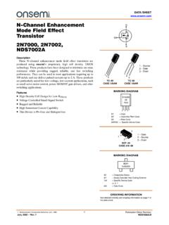
1 DATA Semiconductor Components Industries, LLC, 2010 April, 2022 Rev. 71 Publication Order Number: MMBF170 /DField Effect Transistor -N- channel , EnhancementModeBS170, MMBF170 General DescriptionThese N channel enhancement mode Field Effect transistors areproduced using onsemi s proprietary, high cell density, DMOS technology. These products have been designed to minimize on stateresistance while provide rugged, reliable, and fast switchingperformance. They can be used in most applications requiring up to500 mA DC. These products are particularly suited for low voltage,low current applications such as small servo motor control, powerMOSFET gate drivers, and other switching High Density Cell Design for Low RDS(ON)
2 Voltage Controlled Small Signal Switch Rugged and Reliable High Saturation Current Capability These are Pb Free DevicesMARKING DIAGRAMSee detailed ordering and shipping information on page 6 ofthis data INFORMATIONSOT 23 CASE 318 0816 ZMBS170, 6Z = Device CodeA= Assembly Plant CodeL= Wafer Lot NumberYW= Assembly Start WeekM= Date CodeTO 92 3 LEADFORMEDCASE 135 ARTO 92 3 135 ANBS170 ALYWGateSourceDrainDGSDGSDSGBS170 MMBF170BS170, MAXIMUM RATINGS (TA = 25 C unless otherwise noted)SymbolParameterBS170 MMBF170 UnitVDSSD rain Source Voltage60 VVDGRD rain Gate Voltage (RGS 1 MW)60 VVGSSGate Source Voltage 20 VIDD rain Current Continuous500500mA Pulsed1200800TJ, TSTGO perating and Storage Temperature Range 55 to 150 CTLM aximum Lead Temperature for Soldering Purposes, 1/16 from Casefor 10 Seconds300 CStresses exceeding those listed in the Maximum Ratings table may damage the device.
3 If any of these limits are exceeded, device functionalityshould not be assumed, damage may occur and reliability may be CHARACTERISTICS (TA = 25 C unless otherwise noted)SymbolParameterBS170 MMBF170 UnitPDMaximum Power Dissipation Derate above 25 CRqJAThermal Resistance, Junction to Ambient150417 C/WELECTRICAL CHARACTERISTICS (TA = 25 C unless otherwise noted)SymbolParameterTest ConditionTypeMinTypMaxUnitOFF CHARACTERISTICSBVDSSD rain Source Breakdown VoltageVGS = 0 V, ID = 100 mAAll60 VIDSSZero Gate Voltage Drain CurrentVDS = 25 V, VGS = 0 VAll Body Leakage, ForwardVGS = 15 V, VDS = 0 VAll 10nAON CHARACTERISTICS (Note 1)VGS(th)Gate Threshold VoltageVDS = VGS, ID = 1 (ON)Static Drain Source On ResistanceVGS = 10 V, ID = 200 mAAll TransconductanceVDS = 10 V, ID = 200 mABS170 320 mSVDS 2 VDS(on)
4 , ID = 200 mAMMBF170 320 DYNAMIC CHARACTERISTICSCissInput CapacitanceVDS = 10 V, VGS = 0 V, f = MHzAll 2440pFCossOutput CapacitanceAll 1730pFCrssReverse Transfer CapacitanceAll 710pFSWITCHING CHARACTERISTICS (Note 1)tonTurn On TimeVDD = 25 V, ID = 200 mA, VGS = 10 V, RGEN = 25 WBS170 10nsVDD = 25 V, ID = 500 mA, VGS = 10 V, RGEN = 50 WMMBF170 10toffTurn Off TimeVDD = 25 V, ID = 200 mA, VGS = 10 V, RGEN = 25 WBS170 10nsVDD = 25 V, ID = 500 mA, VGS = 10 V, RGEN = 50 WMMBF170 10 Product parametric performance is indicated in the Electrical Characteristics for the listed test conditions, unless otherwise noted. Productperformance may not be indicated by the Electrical Characteristics if operated under different Pulse Test: Pulse Width 300 ms, Duty Cycle , ELECTRICAL CHARACTERISTICSF igure 1.
5 On Region CharacteristicsFigure 2. On Resistance Variation with GateVoltage and Drain CurrentFigure 3. On Resistance Variation withTemperatureFigure 4. On Resistance Variation withDrain Current and TemperatureFigure 5. Transfer CharacteristicsFigure 6. Gate Threshold Variation withTemperatureBS170, ELECTRICAL CHARACTERISTICS (continued)Figure 7. Breakdown Voltage Variation withTemperatureFigure 8. Body Diode Forward VoltageVariation with Current and TemperatureFigure 9. Capacitance CharacteristicsFigure 10. Gate Charge CharacteristicsFigure 11. Switching Test CircuitFigure 12. Switching WaveformsBS170, ELECTRICAL CHARACTERISTICS (continued)Figure 13.
6 BS170 Maximum Safe OperatingAreaFigure 14. MMBF170 Maximum Safe OperatingAreaFigure 15. TO 92, BS170 Transient Thermal Response CurveFigure 16. SOT 23, MMBF170 Transient Thermal Response CurveBS170, INFORMATIONPart NumberPackageLead FramePin ArrayShipping BS170TO 92(Pb Free)StraightD G S10000 Units / BulkBS170 D26 ZTO 92(Pb Free)FormingD G S2000 / Tape & ReelBS170 D27 ZTO 92(Pb Free)FormingD G S2000 / Tape & ReelBS170 D74 ZTO 92(Pb Free)FormingD G S2000 / AmmoBS170 D75 ZTO 92(Pb Free)FormingD G S2000 / AmmoMMBF170 SOT 23(Pb Free)3000 / Tape & Reel For information on tape and reel specifications, including part orientation and tape sizes, please refer to our Tape and Reel PackagingSpecifications Brochure, BRD8011 92 3 135 ANISSUE ODATE 31 JUL 2016 MECHANICAL CASE OUTLINEPACKAGE DIMENSIONSON Semiconductor and are trademarks of Semiconductor Components Industries, LLC dba ON Semiconductor or its subsidiaries in the United States and/or other Semiconductor reserves the right to make changes without further notice to any products herein.
7 ON Semiconductor makes no warranty, representation or guarantee regardingthe suitability of its products for any particular purpose, nor does ON Semiconductor assume any liability arising out of the application or use of any product or circuit, and specificallydisclaims any and all liability, including without limitation special, consequential or incidental damages. ON Semiconductor does not convey any license under its patent rights nor therights of NUMBER:DESCRIPTION:Electronic versions are uncontrolled except when accessed directly from the Document versions are uncontrolled except when stamped CONTROLLED COPY in 1 OF 1TO 92 3 Semiconductor Components Industries, LLC, 92 3 LEADFORMEDCASE 135 ARISSUE ODATE 30 SEP 2016 MECHANICAL CASE OUTLINEPACKAGE DIMENSIONSON Semiconductor and are trademarks of Semiconductor Components Industries, LLC dba ON Semiconductor or its subsidiaries in the United States and/or other Semiconductor reserves the right to make changes without further notice to any products herein.
8 ON Semiconductor makes no warranty, representation or guarantee regardingthe suitability of its products for any particular purpose, nor does ON Semiconductor assume any liability arising out of the application or use of any product or circuit, and specificallydisclaims any and all liability, including without limitation special, consequential or incidental damages. ON Semiconductor does not convey any license under its patent rights nor therights of NUMBER:DESCRIPTION:Electronic versions are uncontrolled except when accessed directly from the Document versions are uncontrolled except when stamped CONTROLLED COPY in 1 OF 1TO 92 3 LEADFORMED Semiconductor Components Industries, LLC, 23 (TO 236)CASE 318 08 ISSUE ASDATE 30 JAN 2018 SCALE 4:1DA13121 XXXMGGXXX = Specific Device CodeM= Date CodeG= Pb Free Package*This information is generic.
9 Please refer todevice data sheet for actual part Free indicator, G or microdot G ,may or may not be DIAGRAM*NOTES:1. DIMENSIONING AND TOLERANCING PER ASME , CONTROLLING DIMENSION: MAXIMUM LEAD THICKNESS INCLUDES LEAD LEAD THICKNESS IS THE MINIMUM THICKNESS OFTHE BASE DIMENSIONS D AND E DO NOT INCLUDE MOLD FLASH,PROTRUSIONS, OR GATE FOOTPRINTVIEW VIEW 22:PIN 1. RETURN2. OUTPUT3. INPUTSTYLE 6:PIN 1. BASE2. EMITTER3. COLLECTORSTYLE 7:PIN 1. EMITTER2. BASE3. COLLECTORSTYLE 8:PIN 1. ANODE2. NO CONNECTION3. CATHODESTYLE 9:PIN 1. ANODE2. ANODE3. CATHODESTYLE 10:PIN 1.
10 DRAIN2. SOURCE3. GATESTYLE 11:PIN 1. ANODE2. CATHODE3. CATHODE ANODESTYLE 12:PIN 1. CATHODE2. CATHODE3. ANODESTYLE 13:PIN 1. SOURCE2. DRAIN3. GATESTYLE 14:PIN 1. CATHODE2. GATE3. ANODESTYLE 15:PIN 1. GATE2. CATHODE3. ANODESTYLE 16:PIN 1. ANODE2. CATHODE3. CATHODESTYLE 17:PIN 1. NO CONNECTION2. ANODE3. CATHODESTYLE 18:PIN 1. NO CONNECTION2. CATHODE3. ANODESTYLE 19:PIN 1. CATHODE2. ANODE3. CATHODE ANODESTYLE 23:PIN 1. ANODE2. ANODE3. CATHODESTYLE 20:PIN 1. CATHODE2. ANODE3. GATESTYLE 21:PIN 1. GATE2. SOURCE3. DRAINSTYLE 1 THRU 5:CANCELLEDSTYLE 24:PIN 1.