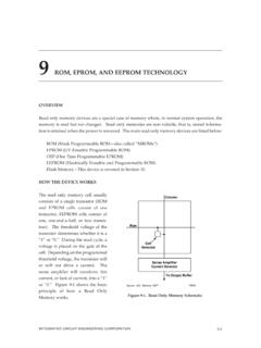
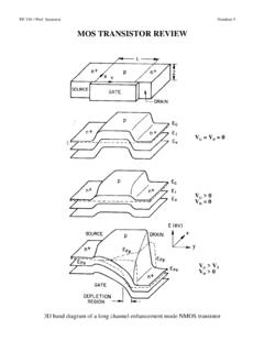
Transcription of NDS7002A - N-Channel Enhancement Mode Field Effect …
1 DATA Semiconductor Components Industries, LLC, 1998 July, 2022 Rev. 71 Publication Order Number: NDS7002A /DN- channel EnhancementMode Field EffectTransistor2N7000, 2N7002,NDS7002 ADescriptionThese N channel Enhancement mode Field Effect transistors areproduced using onsemi s proprietary, high cell density, DMOS technology. These products have been designed to minimize on stateresistance while providing rugged, reliable, and fast switchingperformance. They can be used in most applications requiring up to400 mAdc and can deliver pulsed currents up to 2 A. These productsare particularly suited for low voltage, low current applications, suchas small servo motor control, power MOSFET gate drivers, and otherswitching High Density Cell Design for Low RDS(on)
2 Voltage Controlled Small Signal Switch Rugged and Reliable High Saturation Current Capability This Device is Pb Free and Halogen FreeSee detailed ordering and shipping information on page 7 ofthis data INFORMATIONMARKING DIAGRAMTO 92 CASE 135AN&E= Designates Space&Y= Binary Calendar Year Coding Scheme7x2= Specific Device Codex= 0, 1&G= Date CodeSDG&E&Y7x2&E&GSOT 23 CASE 318 08$Y= Logo&Z= Assembly Plant Code&3= Date Code2N7000 = Specific Device Code$Y&Z&32N7000123123TO 92 CASE 135 ARMARKING DIAGRAM1 Source2 Gate3 Drain1 Gate2 Source3 Drain1232N7000, 2N7002, MAXIMUM RATINGS Values are at TC = 25 C unless otherwise to Source Voltage60 VVDGRD rain Gate Voltage (RGS 1 MW)60 VVGSSGate Source Voltage Continuous 20 VGate Source Voltage Non Repetitive (tp < 50 ms) 40 IDMaximum Drain Current Continuous200115280mAMaximum Drain Current Pulsed5008001500 PDMaximum Power Dissipation Derated above 25 CTJ, TSTGO perating and Storage Temperature Range 55 to 150 65 to 150 CTLM aximum Lead Temperature for Soldering Purposes,1/16 inch from Case for 10 s300 CStresses exceeding those listed in the Maximum Ratings table may damage the device.
3 If any of these limits are exceeded, device functionalityshould not be assumed, damage may occur and reliability may be CHARACTERISTICS Values are at TC = 25 C unless otherwise JAThermal Resistance, Junction to C/WELECTRICAL CHARACTERISTICS Values are at TC = 25 C unless otherwise CHARACTERISTICSBVDSSD rain Source Breakdown VoltageVGS = 0 V, ID = 10 mAAll60 VIDSSZero Gate Voltage Drain CurrentVDS = 48 V, VGS = 0 V2N7000 1mAVDS = 48 V, VGS = 0 V, TC = 125 C 1mAVDS = 60 V, VGS = 0 V2N7002 NDS7002A 1mAVDS = 60 V, VGS = 0 V, TC = 125 C Body Leakage, ForwardVGS = 15 V, VDS = 0 V2N7000 10nAVGS = 20 V, VDS = 0 V2N7002 NDS7002A 100 IGSSRGate Body Leakage, ReverseVGS = 15 V, VDS = 0 V2N7000 10nAVGS = 20 V, VDS = 0 V2N7002 NDS7002A 100ON CHARACTERISTICSVGS(th)Gate Threshold VoltageVDS = VGS, ID = 1 = VGS, ID = 250 , 2N7002, CHARACTERISTICS (continued)Values are at TC = 25 C unless otherwise CHARACTERISTICSRDS(on)
4 Static Drain Source On ResistanceVGS = 10 V, ID = 500 mA2N7000 = 10 V, ID = 500 mA,TC = 125 C = V, ID = 75 mA = 10 V, ID = 500 mA2N7002 = 10 V, ID = 500 mA,TC = 100 C = 5 V, ID = 50 mA = 5 V, ID = 50 mA,TC = 100 C = 10 V, ID = 500 mANDS7002A = 10 V, ID = 500 mA,TC = 125 C = 5 V, ID = 50 mA = 5 V, ID = 50 mA,TC = 125 C (on)Drain Source On VoltageVGS = 10 V, ID = 500 mA2N7000 = V, ID = 75 mA = 10 V, ID = 500 mA2N7002 = V, ID = 50 mA = 10 V, ID = 500 mANDS7002A = V, ID = 50 mA (on)On State Drain CurrentVGS = V, VDS = 10 V2N700075600 mAVGS = 10 V, VDS 2 VDS(on)2N70025002700 VGS = 10 V, VDS 2 VDS(on)NDS7002A5002700 gFSForward TransconductanceVDS = 10 V, ID = 200 mA2N7000100320 mSVDS 2 VDS(on), ID = 200 mA2N700280320 VDS 2 VDS(on)
5 , ID = 200 mANDS7002A80320 DYNAMIC CHARACTERISTICSCissInput CapacitanceVDS = 25 V, VGS = 0 V, f = MHzAll 2050pFCossOutput CapacitanceAll 1125 CrssReverse Transfer CapacitanceAll 45tonTurn On TimeVDD = 15 V, RL = 25 W, ID = 500 mA, VGS = 10 V, RGEN = 25 W2N7000 10nsVDD = 30 V, RL = 150 W, ID = 200 mA, VGS = 10 V,RGEN = 25 W2N7002 NDS7002A 20toffTurn Off TimeVDD = 15 V, RL = 25 W, ID = 500 mA, VGS = 10 V, RGEN = 25 W2N7000 10nsVDD = 30 V, RL = 150 W, ID = 200 mA, VGS = 10 V,RGEN = 25 W2N7002 NDS7002A 202N7000, 2N7002, CHARACTERISTICS (continued)Values are at TC = 25 C unless otherwise SOURCE DIODE CHARACTERISTICS AND MAXIMUM RATINGSISM aximum Continuous Drain Source Diode Forward Current2N7002 115mANDS7002A 280 ISMM aximum Pulsed Drain Source Diode Forward Current2N7002 Source DiodeForward VoltageVGS = 0 V, IS = 115 mA(Note 1)2N7002 = 0 V, IS = 400 mA(Note 1) NDS7002A parametric performance is indicated in the Electrical Characteristics for the listed test conditions, unless otherwise noted.
6 Productperformance may not be indicated by the Electrical Characteristics if operated under different Pulse test: Pulse Width 300 ms, Duty Cycel 2 %TYPICAL PERFORMANCE CHARACTERISTICSF igure 1. On Region CharacteristicsFigure 2. On Resistance Variation withGate Voltage and Drain , Drain Current (A)RDS(on), Normalized Drain Source On ResistanceVDS, Drain Source Voltage (V) = 10 VV = 3. On Resistance Variation withTemperatureFigure 4. On Resistance Variation withDrain Current and Temperature 50 , Drain Current (A)RDS(on), Normalized Drain Source On ResistanceTJ, Junction Temperature (5C) (on), Normalized Drain Source On = 125 C25 C 55 CVGS = 10 VID = 500 mAID, Drain Source Current (A)2N7000, 2N7002, PERFORMANCE CHARACTERISTICS (Continued)Figure 5.
7 Transfer CharacteristicsFigure 6. Gate Threshold Variation , Junction Temperature (5C)Vth, Normalized Gate SourceThreshold VoltageVGS, Gate to Source Voltage (V) , Drain Current (A)810 VDS = 10 VT = 55 C25 C125 C 50 252550075100125 150 VDS = VGSI = 1 mAFigure 7. Breakdown Voltage Variation withTemperatureFigure 8. Body Diode Forward VoltageVariation , Body Diode Forward Voltage (V)IS, Reverse Drain Current (A) , Normalized Drain Source Breakdown 50 252550075100125150ID = 250 mATJ, Junction Temperature (5C) = 0 V25 C 55 CFigure 9. Capacitance CharacteristicsFigure 10. Gate Charge Characteristics121020531251020Qg, Gate Charge (nC)VGS, GA E Source Voltage (V)VDS, Drain to Source Voltage (V)Capacitance (pF) mA280 mAVDS = 25 VI = 500 mAT = 125 Cf = 1 MHzV = 0 , 2N7002, PERFORMANCE CHARACTERISTICS (Continued)Figure 11.
8 Switching Test CircuitFigure 12. Switching WaveformsVGSRGENVINGDVDDRLSDUTVOUTO utput, VoutInput, Vin10%50%50%90%10%90%90%InvertedPulse Width10%td(on)tontrtd(off)tofftfFigure 13. 2N7000 Maximum Safe Operating AreaFigure 14. 2N7002 Maximum Safe Operating , Drain Source Voltage (V)ID, Drain Current (A)1230803 VDS, Drain Source Voltage (V)1210205603080ID, Drain Current (A)100 ms1 15. NDS7000A Maximum Safe Operating Area121020560 VDS, Drain Source Voltage (V)ID, Drain Current (A)308010 ms100 ms1 (on) LimitVGS = 10 VSingle PulseTA = 25 C100 ms10 msDS1 ms100 ms1 s10 sRDS(on) LimitVGS = 10 VSingle PulseTA = 25 C10 s10 ms1 ms100 msVGS = 10 VSingle PulseTA = 25 C10 s1 ms100 msRDS(on) Limit2N7000, 2N7002, PERFORMANCE CHARACTERISTICS (Continued)Figure 16.
9 TO 92, 2N7000 Transient Thermal Response , Time (s)r(t), Normalized Effective Transient Thermal (t) = r(t) * RqJARqJA = (See Datasheet)TJ TA = P * RqJA(t)Duty Cycle, D = t1/t2P(pk)t1t2 Single = 17. SOT 23, 2N7002 / NDS7002A Transient Thermal Response , Time (s)r(t), Normalized Effective Transient Thermal (t) = r(t) * RqJARqJA = (See Datasheet)TJ TA = P * RqJA(t)Duty Cycle, D = t1/t2P(pk)t1t2 Single = INFORMATIONPart NumberMarkingPackagePacking Method Min Order Qty / Immediate Pack Qty2N70002N7000TO 92 3L(Pb Free)Bulk10000 / 10002N7000 D74 ZAmmo2000 / 20002N7000 D75 ZTape and Reel2000 / 20002N7000 D26Z2000 / 20002N7002702 SOT 23 3L(Pb Free)
10 Tape and Reel3000 / 3000 NDS7002A7123000 / 3000 For information on tape and reel specifications, including part orientation and tape sizes, please refer to our Tape and Reel PackagingSpecifications Brochure, BRD8011 92 3 135 ANISSUE ODATE 31 JUL 2016 MECHANICAL CASE OUTLINEPACKAGE DIMENSIONSON Semiconductor and are trademarks of Semiconductor Components Industries, LLC dba ON Semiconductor or its subsidiaries in the United States and/or other Semiconductor reserves the right to make changes without further notice to any products herein. ON Semiconductor makes no warranty, representation or guarantee regardingthe suitability of its products for any particular purpose, nor does ON Semiconductor assume any liability arising out of the application or use of any product or circuit, and specificallydisclaims any and all liability, including without limitation special, consequential or incidental damages.