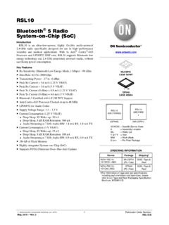
Transcription of RSL10 SIP Bluetooth 5 System-in-Package (SiP)
1 Semiconductor Components Industries, LLC, 2018 May, 2020 Rev. 11 Publication Order Number: RSL10 SIP/DBluetooth) 5 System-in-Package (SiP) RSL10 SIPI ntroductionRSL10 System In Package ( RSL10 SIP) is a complete solutionthat provides the easiest way to integrate the industry s lowest powerBluetooth low energy technology into a wireless RSL10 SIP features an on board antenna, RSL10 radio SoC,and all necessary passive components in one package to help minimizeoverall system size. Already fully qualified to FCC, CE, and otherregulatory standards; RSL10 SIP removes the need for additionalantenna design considerations or RF Features Fully Certified: Bluetooth 5 QDID Declaration ID FCC, CE, IC, MIC, KCC Industry s Lowest Power: Peak Rx Current = mA ( V VBAT) Peak Rx Current = mA (3 V VBAT) Peak Tx Current (0 dBm) = mA ( V VBAT) Peak Tx Current (0 dBm) = mA (3 V VBAT) Deep Sleep Current Consumption ( V VBAT): Deep Sleep, IO Wake up: 50 nA Deep Sleep, 8 kB RAM Retention: 300 nA Current Consumption (3 V VBAT): Deep Sleep, IO Wake up: 25 nA Deep Sleep, 8 kB RAM Retention: 100 nA EEMBC ULPMark Core Profile (3 V): 1090 EEMBC ULPMark Core Profile ( V): 1360 Advanced Wireless: Support for Bluetooth 5 features.
2 LE 2 Mbit PHY (High Speed),as well as backwards compatibility and support for earlierBluetooth Low Energy specifications Supports FOTA (Firmware Over The Air) Updates Rx Sensitivity ( Bluetooth Low Energy Mode, 1 Mbps): 93 dB Transmitting Power: 17 to 0 dBm Range up to 100 MetersOther Key Features Arm Cortex M3 Processor Clocked at up to 48 MHz Supply Voltage Range: V 384 kB of Flash Memory 76 kB of Program Memory 88 kB of Data 8x6 CASE 127 EYXXXXXX = Specific Device CodeA= Assembly LocationWL= Wafer LotY= YearWW= Work WeekG or G= Pb Free PackageDevicePackageShipping ORDERING INFORMATIONNCH RSL10 101S51 ACGSIP51(Pb Free)2500 / Tape & Reel For information on tape and reel specifications,including part orientation and tape sizes, pleaserefer to our Tape and Reel Packaging SpecificationBrochure, BRD8011/D.
3 (SIP51)XXXXXAWLYWWRSL10 Arm Cortex M3 Processor: A 32 bit core forreal time applications, specifically developed to enablehigh performance low cost platforms for a broad rangeof low power applications. LPDSP32: A 32 bit Dual Harvard DSP core thatefficiently supports intensive signal processingapplications. Various codecs are available to customersthrough libraries that are included in RSL10 sdevelopment tools. Radio Frequency Front End: Based on a GHz RFtransceiver, the RFFE implements the physical layer ofthe Bluetooth low energy technology standard and otherproprietary or custom protocols. Protocol Baseband Hardware: Bluetooth 5 certifiedand includes support for a 2 Mbps RF link and customprotocol options.
4 The RSL10 baseband stack issupplemented by support structures that enableimplementation of ON Semiconductor and customerdesigned custom protocols. Highly Integrated SoC: The dual core architecture iscomplemented by high efficiency power managementunits, oscillators, flash and RAM memories, a DMAcontroller, along with a full complement of peripheralsand interfaces. Deep Sleep Mode: RSL10 can be put into a DeepSleep Mode when no operations are required. VariousDeep Sleep Mode configurations are available,including: IO wake up configuration. The powerconsumption in deep sleep mode is 50 nA ( VVBAT). Embedded 32 kHz oscillator running with interruptsfrom timer or external pin. The total current drain is90 nA ( V VBAT).
5 As above with 8 kB RAM data retention. The totalcurrent drain is 300 nA ( V VBAT). The DC DC converter can be used in buck mode orLDO mode during Sleep Mode, depending on VBAT voltage. Standby Mode: Can be used to reduce the averagepower consumption for off duty cycle operation,ranging typically from a few ms to a few hundreds ofms. The typical chip power consumption is 30 mA inStandby Mode. Multi Protocol Support: Using the flexibilityprovided by LPDSP32, the Arm Cortex M3 processor,and the RF front end; proprietary protocols and othercustom protocols are supported. Flexible Supply Voltage: RSL10 integrates high efficiency power regulators and has a VBAT range to V. Highly Configurable Interfaces: , UART, two SPIinterfaces, PCM interface, multiple GPIOs.
6 It alsosupports a digital microphone interface (DMIC) and anoutput driver (OD). Flexible Clocking Scheme: RSL10 must be clockedfrom the XTAL/PLL of the radio front end at 48 MHzwhen transmitting or receiving RF traffic. When RSL10is not transmitting/receiving RF traffic, it can run offthe 48 MHz XTAL, the internal RC oscillators, the32 kHz oscillator, or an external clock. A lowfrequency RTC clock at 32 kHz can also be used inDeep Sleep Mode. It can be sourced from either theinternal XTAL, the RC oscillator, or a digital input pad. Diverse Memory Architecture: 76 kB of SRAM program memory (4 kB of which is PROM containingthe chip boot up program, and is thus unavailable tothe user) and 88 kB of SRAM data memory areavailable.
7 A total of 384 kB of flash is available to storethe Bluetooth stack and other applications. The Arm Cortex M3 processor can execute fromSRAM and/or flash. Security: AES128 encryption hardware block forcustom secure algorithms and code protection withauthenticated debug port access (JTAG lock ) Ultra Low Power Consumption ApplicationExamples: Low Duty Cycle Advertising: IDD mA foradvertising at all three channels at 5 second intervals@ VBAT 3 V, DCDC converter enabled. RoHS Compliant DeviceRSL10 specifications for the RSL10 System in Package arebased on the RSL10 radio SoC. The RSL10 SIP data sheetonly contains key parameters. For a full list of RSL10parameters and specifications, refer to the RSL10 data Board ConnectionThe RSL10 SIP is designed to be reflowed onto low costprinted circuit boards.
8 The RSL10 SIP connects to theapplication board via solder pads located on the properly operate the RSL10 SIP an external PCBconnection between the RF and ANT pads is required. Thisconnection connects the RF pin on RSL10 to the antennainside the SiP. If an external antenna is used instead of theantenna internal to the SiP, this external antenna needs to beconnected to PIN , an external PCB connection is required forthe VDDO pad to ensure that it is not left floating. Forexample, it can be connected to VBAT so that the logic highlevel for the digital I/O (DIO) pads is equal to 1 and 2 show proposed layout patterns for theRSL10 SIP. The specific layout pattern used in theapplication may have to be adjusted to meet certain needs ofthe PCB manufacturer or assembly house.
9 PCB design filesfor the RSL10 SIP are available at 1. RSL10 SIP Keepout Area RequirementsNotes:1. Align component edge to PCB edge if Extend keepout area to PCB Keepout area All Keepout area Top layer Units = 2. Minimum Top Layer Ground StructureNotes:1. When incorporating internal antenna, join landing pads using x Establish 50 W impedance to underlying reference Maintain minimum 300 mm distance from ground Area for several Refer to radiation efficiency data for applicable ground plane Units = SiP SchematicThe schematic for the RSL10 SIP is shown in Figure 3. RSL10 SIP SchematicFigure 4. Pin Connection DiagramRSL10 FUNCTION DESCRIPTIONFor detailed pad function information see the RSL10 data 1.
10 PAD LIST Pad IdentifierPad NameI/OA/DPullDescriptionA1 JTMSI/ODUCM3 JTAG Test Mode StateA2 DOI12I/ODU/DDigital input output 12A3 JTCKI/ODUCM3 JTAG Test ClockA4 DOI10I/ODU/DDigital input output 10A5 DOI6I/ODU/DDigital input output 6A6 DOI3I/OA/DU/DDigital input output 3 / ADC 3A7 DOI2I/OA/DU/DDigital input output 2 / ADC 2A8 DOI5I/ODU/DDigital input output 5B1 DOI13I/ODU/DDigital input output/CM3 JTAG Test ResetB2 DOI14I/ODU/DDigital input output/CM3 JTAG Test Data InB3 DOI11I/ODU/DDigital input output 11B5 DOI8I/ODU/DDigital input output 8B6 DOI1I/OA/DU/DDigital input output 1 / ADC 1B7 DOI7I/ODU/DDigital input output 7B8 DOI4I/ODU/DDigital input output 4C1 DOI15I/ODU/DDigital input output/CM3 JTAG Test Data OutC2 DOI9I/ODU/DDigital input output 9C7 DOI0I/OA/DU/DDigital input output 0 / ADC 0C8 EXT_CLKIDUE xternal clock inputD1 DGNDI/OPGroundD2 DGNDI/OPGroundD7 VDDOIPD igital O/I voltage supplyD8 VBATIPB attery input voltageE1 RFI/OARF signal input/outputE2 DGNDI/OPGroundE7 NRESETIDUR eset pinE8 AOUTOAA nalog test pinF1 ANTI/OAAntennaF2 DGNDI/OPGroundF3 DGNDI/OPGroundF4 DGNDI/OPGroundF5 DGNDI/OPGroundF6 DGNDI/OPGroundF7 RESIDDRESERVEDF8 WAKEUPIAWake up pin for power modesG1 DGNDI/OPGroundG2 DGNDI/OPGroundG3 DGNDI/OPGroundG4 DGNDI/OPGroundG5 DGNDI/OPGroundRSL10 1.